 ChipApex | Global Electronic Components Supplier
SEARCH
Search Product
Search Post
— IC芯片 | 连接器 | 传感器 | 被动器件 —
Search productSearch post
— IC芯片 | 连接器 | 传感器 | 被动器件 —
Consult the customer manager about the wholesale price.
consultation hotline:86-132-6715-2157
email:[email protected]
Contact the product manager for consultation. One-stop consultation is available.
Do you want a lower wholesale price? Please send us your inquiry and we will reply immediately.
The 8S89296NLGI is a high-performance LVDS programmable delay line manufactured by Renesas Electronics Corporation. It features one differential clock input pair and one LVDS level output. The device operates on a full 2.5V supply voltage and supports an input maximum frequency of 800MHz. The programmable delay range spans from 2.2ns to 12.5ns, adjustable in discrete 10ps steps via a 10-bit control word. The D[10:0] pins accept LVPECL, LVCMOS, or LVTTL levels, while the control register accepts CMOS or TTL signals. It is characterized for operation within an ambient temperature range of -40 °C to +85 °C.
Verify the specific suffix NLGI against official Renesas documentation to confirm package type and tape/reel specifications. Ensure compatibility with 2.5V supply requirements and LVDS signal integrity standards for your design. Confirm RoHS compliance status as indicated in the datasheet. Cross-reference pinout details with the official outline drawing before PCB layout finalization.
Select this component when precise sub-nanosecond delay adjustments are required for LVDS clock signals. Verify that the system operates at 2.5V and requires support for LVPECL, LVDS, or CML inputs. Consider the 10-bit resolution for delay granularity needs. Ensure the operating temperature range meets the application environment constraints.
The 8S89296 series belongs to Renesas' portfolio of high-performance clock management ICs. These devices are designed for applications demanding accurate skew control and jitter performance. The NLGI variant specifies the particular package and packaging configuration available through authorized channels.
Consult official Renesas substitution guides for verified alternatives. Generic delay lines may not match the specific LVDS input/output characteristics or 10ps step resolution. Verify electrical compatibility before considering cross-brand replacements.


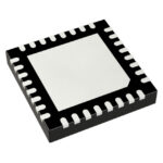 8S89296NLGI
The activity of extra discounts on wholesale prices is in full swing…
Please fill in your contact information and we will send you the latest wholesale price list.




