 ChipApex | Global Electronic Components Supplier

SEARCH
Search Product
Search Post
— IC芯片 | 连接器 | 传感器 | 被动器件 —
Search productSearch post
— IC芯片 | 连接器 | 传感器 | 被动器件 —
Consult the customer manager about the wholesale price.
consultation hotline:86-132-6715-2157
email:[email protected]
Contact the product manager for consultation. One-stop consultation is available.
Do you want a lower wholesale price? Please send us your inquiry and we will reply immediately.
8SLVD1212ANLGI/W is listed in the Clock Buffers, Drivers range at ChipApex. The manufacturer field lists Renesas Electronics Corporation. Its product description is IC CLK BUFFER 1:2 3GHZ 40VFQN. Review the specifications below when checking this part for your BOM.
The 8SLVD1212ANLGI/W is a high-performance, 12-output differential LVDS fanout buffer manufactured by Renesas Electronics. Designed for clock distribution applications requiring low additive phase noise and well-defined skew characteristics, the device operates from a single 2.5V power supply. It features two selectable differential inputs capable of accepting LVDS, LVPECL, or CML signal levels. The component integrates bias voltage generators to facilitate interfacing with single-ended signals. Characterized for operation within an ambient temperature range of -40°C to +85°C, it is housed in a lead-free (RoHS 6 compliant), 40-lead VFQFN package measuring 6.0 x 6.0 mm.
This component belongs to the 8SLVP family of fanout buffers. It shares architectural similarities with other devices in the series, such as the 8SLVP1212I, but is specifically optimized for LVDS output standards rather than LVPECL. The 'NLGI' suffix indicates a specific tape and reel packaging configuration suitable for automated surface-mount assembly.
Direct pin-to-pin replacements within the same family include the 8SLVP1212I, though this variant utilizes LVPECL outputs instead of LVDS. Designers must verify output voltage compatibility when substituting between LVDS and LVPECL variants. Other members of the 8SLVP series may offer different output counts or input configurations.
Explore related parts through Clock/Timing, Integrated Circuits (ICs), all product categories, ChipApex homepage.
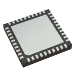 8SLVD1212ANLGI/W

The activity of extra discounts on wholesale prices is in full swing…
Please fill in your contact information and we will send you the latest wholesale price list.






