 ChipApex | Global Electronic Components Supplier
8T49N240-025NLGI
Search Product
Search Post
— IC芯片 | 连接器 | 传感器 | 被动器件 —
Search productSearch post
— IC芯片 | 连接器 | 传感器 | 被动器件 —
Consult the customer manager about the wholesale price.
consultation hotline:86-132-6715-2157
email:[email protected]
Contact the product manager for consultation. One-stop consultation is available.
Do you want a lower wholesale price? Please send us your inquiry and we will reply immediately.
The 8T49N240-025NLGI is a clock synthesizer and jitter attenuator from Renesas Electronics, part of the FemtoClock NG family. It operates within a supply voltage range of 2.375 V to 3.465 V and supports an operating temperature range of -40 °C to +85 °C. The device features four output channels with a maximum output frequency of 867 MHz and accepts input frequencies up to 875 MHz. It is housed in a 40-pin VFQFN package and draws approximately 40 mA during operation.
Verify component authenticity through authorized distributors or direct manufacturer channels. Confirm specific order codes match required frequency configurations. Check for moisture sensitivity handling requirements due to the VFQFN package type. Ensure compatibility with existing I2C bus voltages and levels before integration into final designs.
Select this model when four differential or single-ended outputs are required with high-frequency capabilities up to 867 MHz. Consider the VFQFN-40 package constraints for PCB layout and thermal management. Verify that the 875 MHz maximum input frequency meets system reference clock specifications. Evaluate power consumption against available supply rails within the 2.375 V to 3.465 V range.
This component belongs to the 8T49N240 series, designed as low-jitter clock generators. It serves as a replacement for older clock solutions in high-performance networking and computing applications. The 'NLGI' suffix typically denotes specific packaging and tape/reel quantities, while the numeric code defines factory pre-programmed frequency settings.
Direct substitutes may include other models from the 8T49N24x series with compatible pinouts and electrical characteristics. Verify output voltage levels and package dimensions before swapping. Consult Renesas documentation for equivalent part numbers offering similar jitter performance and output configurations.
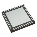 8T49N240-025NLGI
The activity of extra discounts on wholesale prices is in full swing…
Please fill in your contact information and we will send you the latest wholesale price list.





