 ChipApex | Global Electronic Components Supplier
8T49N240-029NLGI
Search Product
Search Post
— IC芯片 | 连接器 | 传感器 | 被动器件 —
Search productSearch post
— IC芯片 | 连接器 | 传感器 | 被动器件 —
Consult the customer manager about the wholesale price.
consultation hotline:86-132-6715-2157
email:[email protected]
Contact the product manager for consultation. One-stop consultation is available.
Do you want a lower wholesale price? Please send us your inquiry and we will reply immediately.
The Renesas 8T49N240-029NLGI is a FemtoClock NG Universal Frequency Translator featuring a single fractional-feedback PLL. It generates up to four independent output frequencies ranging from 8 kHz to 867 MHz using integer and fractional dividers. The device supports LVDS, LVPECL, or HCSL differential outputs with RMS phase jitter below 200 fs (12 kHz to 20 MHz). It accepts dual clock inputs and an internal crystal oscillator, configurable via I²C or OTP memory for jitter attenuation or synthesis modes.
Verify the specific suffix '029' against official Renesas documentation to confirm factory pre-programmed frequency configurations. Confirm current manufacturing status as some 8T49N240 variants are discontinued. Ensure compatibility with required output voltage levels and package specifications before procurement.
Select this component when low phase jitter below 200 fs is required for high-speed serial interfaces. Verify that the maximum output frequency of 867 MHz meets system requirements. Confirm support for desired output formats such as LVDS or LVPECL. Check if the integrated PLL flexibility reduces the need for external fanout buffers.
This part belongs to the Renesas FemtoClock NG family of universal frequency translators. These devices integrate advanced PLL technology to provide flexible clock generation and jitter cleaning. The 8T49N240 series is designed for high-performance networking and telecommunications applications requiring precise timing synchronization.
The 8T49N241 and 8T49N242 are similar devices within the same product family. Verify pin-to-pin compatibility and register configuration differences. Note that Renesas timing products have been acquired by SiTime; consult updated documentation for long-term supply availability.
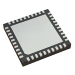 8T49N240-029NLGI
The activity of extra discounts on wholesale prices is in full swing…
Please fill in your contact information and we will send you the latest wholesale price list.






