 ChipApex | Global Electronic Components Supplier
8T49N240-991NLGI8
Search Product
Search Post
— IC芯片 | 连接器 | 传感器 | 被动器件 —
Search productSearch post
— IC芯片 | 连接器 | 传感器 | 被动器件 —
Consult the customer manager about the wholesale price.
consultation hotline:86-132-6715-2157
email:[email protected]
Contact the product manager for consultation. One-stop consultation is available.
Do you want a lower wholesale price? Please send us your inquiry and we will reply immediately.
The 8T49N240-991NLGI8 is a FemtoClock NG Universal Frequency Translator manufactured by Renesas Electronics. It features a single fractional-feedback PLL capable of jitter attenuation or frequency synthesis, equipped with four integer output dividers to generate up to four independent frequencies ranging from 8 kHz to 867 MHz. The device accepts differential inputs including LVPECL, LVDS, and HCSL, and supports crystal inputs between 19.6 MHz and 27.2 MHz. It operates on a 3.3 V supply within a -40°C to +85°C temperature range.
Verify the specific suffix '991' against official Renesas documentation to confirm exact factory pre-programmed configurations. Confirm package type and RoHS compliance status prior to integration. Ensure design-in tools like Timing Commander are available for final validation.
Select this component when low phase jitter performance below 200 fs is required for high-speed interfaces. Consider its small 6 mm x 6 mm footprint for space-constrained layouts. Evaluate its flexibility for replacing multiple fixed-frequency generators with a single programmable solution.
This part belongs to the FemtoClock NG family, designed for high-performance clock generation. It addresses the need for precise timing in multi-gigabit serial links. The series emphasizes low noise and high configurability for modern communication infrastructure.
Consult official substitution lists for compatible devices such as the 8T49N241 or 8T49N242 series. Verify pinout and register compatibility before swapping components in existing designs.
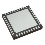 8T49N240-991NLGI8
The activity of extra discounts on wholesale prices is in full swing…
Please fill in your contact information and we will send you the latest wholesale price list.






