 ChipApex | Global Electronic Components Supplier
8T49N240-998NLGI
Search Product
Search Post
— IC芯片 | 连接器 | 传感器 | 被动器件 —
Search productSearch post
— IC芯片 | 连接器 | 传感器 | 被动器件 —
Consult the customer manager about the wholesale price.
consultation hotline:86-132-6715-2157
email:[email protected]
Contact the product manager for consultation. One-stop consultation is available.
Do you want a lower wholesale price? Please send us your inquiry and we will reply immediately.
The 8T49N240-998NLGI is a FemtoClock NG ultra-performance jitter attenuator manufactured by Renesas Electronics. It features one fractional-feedback PLL and four integer output dividers, supporting up to four independent differential or single-ended outputs. The device accepts input frequencies from 8 kHz to 875 MHz and generates output frequencies ranging from 8 kHz to 867 MHz. It operates on a supply voltage between 2.375 V and 3.465 V within an industrial temperature range of -40°C to +85°C. Packaged in a 40-VFQFN exposed pad, it supports I2C programming and booting from external EEPROM.
Verify the specific suffix '998' indicates the configuration for booting from an external I2C EEPROM upon power-up. Confirm package details are 40-VFQFN with an exposed pad. Ensure compatibility with the required supply voltage range of 2.375 V to 3.465 V for the target design.
Select this component when low jitter performance is critical for high-speed serial links. Compare against the 8T49N242 if higher output frequencies up to 1 GHz are required. Verify that the maximum input frequency of 875 MHz meets the source clock requirements of the system.
This part belongs to the FemtoClock NG family of universal frequency translators. It is designed to replace crystal oscillators and VCXOs in complex timing architectures. The device integrates programmable logic to simplify board layout and reduce component count in multi-clock systems.
The 8T49N240-990NLGI is a related variant within the same series. Check datasheets for differences in packaging quantities or specific feature enablement before substitution.
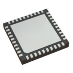 8T49N240-998NLGI
The activity of extra discounts on wholesale prices is in full swing…
Please fill in your contact information and we will send you the latest wholesale price list.





