 ChipApex | Global Electronic Components Supplier
8T49N241-998NLGI#
Search Product
Search Post
— IC芯片 | 连接器 | 传感器 | 被动器件 —
Search productSearch post
— IC芯片 | 连接器 | 传感器 | 被动器件 —
Consult the customer manager about the wholesale price.
consultation hotline:86-132-6715-2157
email:[email protected]
Contact the product manager for consultation. One-stop consultation is available.
Do you want a lower wholesale price? Please send us your inquiry and we will reply immediately.
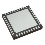
The Renesas 8T49N241-998NLGI is a FemtoClock NG Universal Frequency Translator featuring one fractional-feedback PLL and four output dividers. It generates up to four independent clocks from 8kHz to 1GHz (LVPECL/LVDS/HCSL) or 250MHz (LVCMOS). The device supports I²C programming and boot configuration from an external EEPROM. Key electrical parameters include a maximum input frequency of 875 MHz, a jitter specification of 350 fs RMS (12kHz–20MHz), and operation within a -40°C to +85°C temperature range.
Verify component authenticity through authorized channels as this part number may be subject to obsolescence notices. Confirm package integrity and moisture sensitivity level handling procedures prior to assembly. Cross-reference specific ordering suffixes to ensure compatibility with required boot modes and pinout configurations.
Select this model when requiring four independent clock outputs derived from a single PLL source. Ensure the design accommodates the 40-VFQFN exposed pad package requirements. Verify that the application requires the specific 0.35 ps jitter profile and that the 875 MHz maximum input frequency meets system synchronization needs.
This component belongs to the FemtoClock NG Universal Frequency Translator family. It serves as a versatile clock generator capable of translating various input frequencies into high-performance output clocks suitable for demanding telecommunications and data communication infrastructure environments.
Publicly documented substitutes include the 8T49N241-994NLGI, 8T49N241-998NLGI, and 8T49N242-998NLGI8. Verify functional equivalence regarding output count and voltage levels before substitution.
 8T49N241-998NLGI#
The activity of extra discounts on wholesale prices is in full swing…
Please fill in your contact information and we will send you the latest wholesale price list.





