ChipApex | Global Electronic Components Supplier
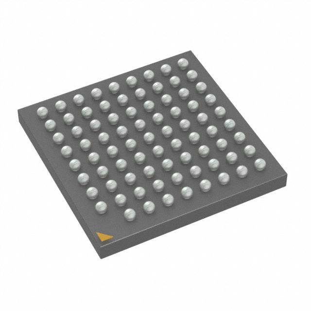
8T49N244A-000ASGI8
Search Product
Search Post
— IC芯片 | 连接器 | 传感器 | 被动器件 —
Search productSearch post
— IC芯片 | 连接器 | 传感器 | 被动器件 —
Consult the customer manager about the wholesale price.
consultation hotline:86-132-6715-2157
email:[email protected]
Contact the product manager for consultation. One-stop consultation is available.
Do you want a lower wholesale price? Please send us your inquiry and we will reply immediately.
The Renesas 8T49N244A-000ASGI8 is a FemtoClock NG Universal Frequency Translator featuring two independent Phase-Locked Loops (PLL-A and PLL-B). It supports low-bandwidth jitter attenuation with manual pin-based switchover. The device accepts differential inputs such as LVPECL, LVDS, HCSL, or LVCMOS, and generates up to four outputs in LVDS format. Key electrical parameters include a maximum output frequency of 1.3 GHz, an input frequency range of 8 kHz to 710 MHz, and a typical RMS phase jitter of 465 fs. It operates on a single 2.5 V supply within a -40°C to +85°C temperature range.
Verify the specific ordering suffix against the official IDT/Renesas FemtoClock UFT Ordering Guide to confirm the exact input/output frequency configuration and boot method. Confirm that the required configuration matches the factory-programmed settings for the -000 code, as custom configurations require direct contact with the manufacturer.
Select this component when dual independent clock domains are required with low-bandwidth jitter filtering. Ensure the application utilizes manual pin-based switching rather than I2C control. Verify that the target output signaling levels match the LVDS specification provided in the datasheet.
This part belongs to the 8T49N244I family of Universal Frequency Translators. It is functionally related to other devices in the series such as the 8T49N366I and 8T49N445I, which offer different numbers of PLLs and output banks but share similar FemtoClock NG technology and interface protocols.
Publicly confirmed substitute part numbers are not available in the provided documentation. Contact the manufacturer for alternative recommendations if this discontinued or legacy part is no longer suitable.
 8T49N244A-000ASGI8
The activity of extra discounts on wholesale prices is in full swing…
Please fill in your contact information and we will send you the latest wholesale price list.