 ChipApex | Global Electronic Components Supplier
8T49N281C-999NLGI
Search Product
Search Post
— IC芯片 | 连接器 | 传感器 | 被动器件 —
Search productSearch post
— IC芯片 | 连接器 | 传感器 | 被动器件 —
Consult the customer manager about the wholesale price.
consultation hotline:86-132-6715-2157
email:[email protected]
Contact the product manager for consultation. One-stop consultation is available.
Do you want a lower wholesale price? Please send us your inquiry and we will reply immediately.
The 8T49N281C-999NLGI is a FemtoClock NG Ultra-Femto Jitter Clock Translator manufactured by Renesas Electronics. It operates within a supply voltage range of 2.375 V to 3.465 V, supporting standard 2.5 V and 3.3 V systems. The device features one circuit with an input-to-output ratio of 1:8, providing eight output channels. Output types include LVCMOS, LVDS, and LVPECL. It is housed in a 56-VFQFN exposed pad package (8x8 mm) designed for surface mount installation. The component supports divider and multiplier functions and operates reliably across a temperature range of -40°C to +85°C.
Verify the specific ordering suffix to ensure compatibility with required packaging and tape-and-reel specifications. Confirm that the 56-VFQFN footprint matches the target PCB layout dimensions. Check for any recent Product Change Notices regarding manufacturing site updates or material composition changes. Ensure the selected variant meets the necessary humidity sensitivity levels for the assembly process. Validate that the supply voltage requirements align with the target system power rails before finalizing procurement.
Select this component when ultra-low jitter performance is critical for high-speed data transmission integrity. Choose the 8T49N281C-999NLGI for designs requiring a single-input to eight-output clock translation architecture. Consider the available output drive options such as LVDS or LVPECL if differential signaling is preferred over single-ended LVCMOS. Evaluate the thermal dissipation requirements associated with the exposed pad VFQFN package for the specific application environment.
This part belongs to the Renesas FemtoClock NG family, which specializes in clock generators and translators. The 8T49N281C series is engineered for applications demanding superior phase noise and jitter reduction. It serves as a key enabling component for modern high-bandwidth digital systems where signal integrity is paramount. The device integrates advanced PLL technology to clean and distribute reference clocks efficiently.
Direct substitutes within the same family include the 8T49N281C-003NLGI and 8T49N281C-005NLGI. These variants share identical pinouts and functional characteristics but may differ in specific jitter performance metrics or output configuration options. Verify that the alternative part number satisfies the exact electrical parameters required by the design before substitution.
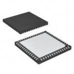 8T49N281C-999NLGI
The activity of extra discounts on wholesale prices is in full swing…
Please fill in your contact information and we will send you the latest wholesale price list.





