 ChipApex | Global Electronic Components Supplier
8T49N282C-999NLGI
Search Product
Search Post
— IC芯片 | 连接器 | 传感器 | 被动器件 —
Search productSearch post
— IC芯片 | 连接器 | 传感器 | 被动器件 —
Consult the customer manager about the wholesale price.
consultation hotline:86-132-6715-2157
email:[email protected]
Contact the product manager for consultation. One-stop consultation is available.
Do you want a lower wholesale price? Please send us your inquiry and we will reply immediately.
The 8T49N282C-999NLGI is a FemtoClock NG Octal Universal Frequency Translator manufactured by Renesas Electronics. It features two independent fractional-feedback PLLs capable of jitter attenuation and frequency translation. The device generates up to eight output frequencies ranging from 8kHz to 1GHz using six integer and two fractional output dividers. It accepts up to four differential or single-ended input clocks and supports LVPECL, LVDS, or LVCMOS output levels. Key electrical parameters include an initial holdover accuracy of ±50ppb, programmable loop bandwidth from 0.5Hz to 512Hz, and RMS phase jitter below 0.3ps (including spurs) for differential outputs in the 12kHz to 20MHz range.
Verify the specific ordering suffix '999' against the manufacturer's datasheet to confirm factory pre-programmed configuration settings. Confirm package type is 72QFN and operating temperature range is -40°C to 85°C. Ensure compatibility with required supply voltages (VCC/VCCA/VCCO).
Select this component when dual independent clock domains are required for separate transmit and receive paths. Verify that the input frequency range (up to 875MHz) and output requirements (up to 1GHz) align with system specifications. Consider the need for gapped clock support and specific jitter attenuation limits for 100G Ethernet or STM-256 applications.
The 8T49N282 belongs to the FemtoClock NG family of universal frequency translators. Originally developed by Integrated Device Technology (IDT), the product line was acquired by Renesas Electronics. This specific model provides octal output capabilities with advanced phase alignment and low-jitter performance suitable for high-speed serial communication standards.
Consult official cross-reference documentation for pin-compatible alternatives within the 8T49N2xx series. Verify that any substitute maintains the same 72QFN package dimensions and electrical characteristics for direct replacement.
The differential outputs meet jitter limits of less than 0.3ps RMS (including spurs) in the 12kHz to 20MHz range.
The device monitors all inputs for Loss of Signal (LOS) and supports automatic or manual hitless switching to redundant backup clocks. If no valid input remains, it enters holdover mode with an initial accuracy of ±50ppb.
Yes, the device can act as a frequency synthesizer where the PLLs generate operating frequencies from the crystal input alone, without requiring external clock references.
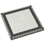 8T49N282C-999NLGI
The activity of extra discounts on wholesale prices is in full swing…
Please fill in your contact information and we will send you the latest wholesale price list.






