 ChipApex | Global Electronic Components Supplier
8T49N286A-998NLGI8
Search Product
Search Post
— IC芯片 | 连接器 | 传感器 | 被动器件 —
Search productSearch post
— IC芯片 | 连接器 | 传感器 | 被动器件 —
Consult the customer manager about the wholesale price.
consultation hotline:86-132-6715-2157
email:[email protected]
Contact the product manager for consultation. One-stop consultation is available.
Do you want a lower wholesale price? Please send us your inquiry and we will reply immediately.
The Renesas 8T49N286A-998NLGI8 is a FemtoClock NG Octal Universal Frequency Translator featuring two independent fractional-feedback PLLs. It accepts up to four differential or single-ended input clocks and a crystal, generating eight output frequencies ranging from 8kHz to 1GHz. The device supports LVPECL, LVDS, HCSL, and LVCMOS output levels. Key electrical parameters include an operating voltage range of 2.375V to 3.465V, an initial holdover accuracy of ±50ppb, and typical jitter performance of <0.3ps RMS (12kHz to 20MHz). It operates within an ambient temperature range of -40°C to +85°C.
Verify the specific ordering suffix against the manufacturer's current datasheet to confirm package type and temperature grade. Confirm availability status as supply conditions may vary. Ensure compatibility with required I2C or SPI programming interfaces and external EEPROM configurations if autonomous loading is needed.
Select this component when multiple independent output frequencies are required from diverse input sources. Verify that the desired output voltage levels (LVPECL, LVDS, HCSL, or LVCMOS) match the system requirements. Check if the specific frequency translation ratios require exact conversion error handling or if standard fractional synthesis is sufficient.
This part belongs to the Renesas FemtoClock NG family, designed for high-performance timing applications. It serves as a universal frequency translator capable of handling various synchronization standards including ITU-T G.709. The device integrates both jitter cleaning and frequency translation capabilities in a single 72-pin QFN package.
Public confirmed substitute part numbers are not available in the provided documentation. Consult the manufacturer's obsolescence notices or cross-reference guides for potential alternatives if this specific variant is discontinued.
The device supports an initial holdover accuracy of ±50ppb for each PLL path when entering holdover state.
Yes, the device monitors all input clocks for Loss of Signal and supports configuration for gapped or ungapped clock operation.
The 8T49N286A contains two independent fractional-feedback PLLs that can lock to different input clocks.
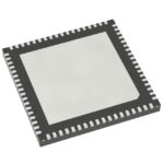 8T49N286A-998NLGI8
The activity of extra discounts on wholesale prices is in full swing…
Please fill in your contact information and we will send you the latest wholesale price list.





