 ChipApex | Global Electronic Components Supplier
8T49N286A-999NLGI8
Search Product
Search Post
— IC芯片 | 连接器 | 传感器 | 被动器件 —
Search productSearch post
— IC芯片 | 连接器 | 传感器 | 被动器件 —
Consult the customer manager about the wholesale price.
consultation hotline:86-132-6715-2157
email:[email protected]
Contact the product manager for consultation. One-stop consultation is available.
Do you want a lower wholesale price? Please send us your inquiry and we will reply immediately.
The 8T49N286A-999NLGI8 is a universal frequency translator from the FemtoClock NG series, manufactured by Renesas Electronics. It operates within a supply voltage range of 2.375V to 3.465V and supports a maximum output frequency of 1GHz. The device features a 5:8 input-to-output ratio with differential input and output capabilities. Input formats include HCSL, LVCMOS, LVDSM, LVHSTL, LVPECL, and crystal references. Output configurations support HSCL, LVCMOS, LVDS, and LVPECL standards. It is housed in a 72-VFQFN exposed pad package (10x10mm) and functions as a single-circuit clock generator.
Verify the specific order code suffix against the official datasheet to ensure correct factory pre-programming. The component requires an external crystal or reference clock source depending on the selected configuration. Confirm moisture sensitivity level (MSL 3) handling requirements during storage and assembly processes.
Select this part when a 5:8 fanout ratio with mixed signal level translation is required. Ensure the design accommodates the 72-VFQFN thermal pad for adequate heat dissipation. Verify that the target application frequency does not exceed the 1GHz maximum limit and that power supply noise meets the jitter specifications.
This component belongs to the 8T49N286 family, which provides universal frequency translation capabilities. The '999' suffix typically denotes a specific factory pre-programmed configuration for standard frequencies. It serves as a replacement for legacy clock generators requiring high flexibility in input/output format conversion.
Direct pin-compatible replacements may exist within the same FemtoClock NG family, such as other 8T49N286 variants with different order codes. Verify register compatibility if migrating between devices with similar form factors but different internal configurations.
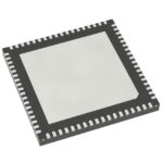 8T49N286A-999NLGI8
The activity of extra discounts on wholesale prices is in full swing…
Please fill in your contact information and we will send you the latest wholesale price list.





