ChipApex | Global Electronic Components Supplier
8T49N366A-000ASGI8
Search Product
Search Post
— IC芯片 | 连接器 | 传感器 | 被动器件 —
Search productSearch post
— IC芯片 | 连接器 | 传感器 | 被动器件 —
Consult the customer manager about the wholesale price.
consultation hotline:86-132-6715-2157
email:[email protected]
Contact the product manager for consultation. One-stop consultation is available.
Do you want a lower wholesale price? Please send us your inquiry and we will reply immediately.
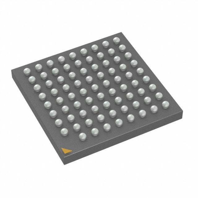
The 8T49N366A-000ASGI8 is a Universal Frequency Translator IC from the FemtoClock NG family, manufactured by Renesas Electronics. It integrates three fully independent Phase-Locked Loops (PLLs) for frequency translation and jitter attenuation. The device supports input frequencies ranging from 8 kHz to 710 MHz and generates programmable output frequencies up to 1.3 GHz. It accepts multiple input signaling formats including LVPECL, LVDS, HCSL, and LVCMOS, while providing differential LVPECL or LVDS outputs. Powered by dual voltage supplies of 2.5V and 3.3V, it operates within an ambient temperature range of -40°C to +85°C in a lead-free 80-pin CABGA package.
This component is marked as obsolete with a Last Time Buy date of May 30, 2025. Verification of current stock availability through authorized distributors is required before procurement planning. Designers should initiate replacement strategies immediately due to the discontinuation status.
Select this part when three independent clock domains are required from a single package. Ensure input signals match supported logic levels (LVPECL/LVDS/HCSL). Verify that the required output frequencies fall within the 0.98 MHz to 1.3 GHz range. Confirm compatibility with the 80-CABGA (10x10 mm) footprint during PCB layout.
The 8T49N366A belongs to the 8T49N366I Universal Frequency Translator family. It shares architectural similarities with the dual-PLL 8T49N244I and quad-PLL 8T49N445I devices. The 'A' suffix typically denotes specific configuration or revision details within the FemtoClock NG series, distinct from the base 'I' designation.
Due to the obsolete status, direct substitutes must be sourced from the same manufacturer's updated portfolio. Consider the 8T49N244A for dual-PLL requirements or 8T49N445A for quad-PLL needs. Cross-reference pinouts and electrical specifications carefully to ensure functional equivalence in existing designs.
 8T49N366A-000ASGI8
The activity of extra discounts on wholesale prices is in full swing…
Please fill in your contact information and we will send you the latest wholesale price list.