 ChipApex | Global Electronic Components Supplier

SEARCH
Search Product
Search Post
— IC芯片 | 连接器 | 传感器 | 被动器件 —
Search productSearch post
— IC芯片 | 连接器 | 传感器 | 被动器件 —
Consult the customer manager about the wholesale price.
consultation hotline:86-132-6715-2157
email:[email protected]
Contact the product manager for consultation. One-stop consultation is available.
Do you want a lower wholesale price? Please send us your inquiry and we will reply immediately.
9DB106BGILFT is listed in the Application Specific Clock/Timing range at ChipApex. The manufacturer field lists Renesas Electronics Corporation. Its product description is IC BUFFER ZD 6OUTPUT 28-TSSOP. Review the specifications below when checking this part for your BOM.
The 9DB106BGILFT is a clock buffer manufactured by Renesas Electronics, designed for PCI Express Gen2 applications. It features six outputs and operates within a supply voltage range of 3.135 V to 3.465 V. The device supports a maximum input frequency of 105 MHz with a maximum propagation delay of 150 ps. It utilizes an LVCMOS input type and provides HCSL output signaling. The component is housed in a TSSOP-28 package and is rated for industrial operating temperatures from 0°C to +70°C.
Verify the specific suffix 'ILFT' against official Renesas documentation to confirm package details and RoHS compliance status. Ensure that the TSSOP-28 package dimensions match the target PCB footprint requirements before finalizing procurement decisions.
Select this component when a six-channel fanout solution is required for PCIe Gen2 architectures. Compare the 105 MHz frequency limit and HCSL output swing against receiver specifications. Verify thermal performance within the 0°C to +70°C operating range for the intended environment.
This part belongs to the 9DB106 series of clock buffers. It serves as a successor or variant to earlier models like the 9DB106BFLF, which has been marked as obsolete. The series provides zero-delay buffering capabilities for high-speed serial interfaces.
The 9DB106BGLF is listed as a similar alternative to the discontinued 9DB106BFLF. Verify electrical pinouts and timing parameters between the ILFT and other suffix variants before substitution.
Explore related parts through Clock/Timing, Integrated Circuits (ICs), all product categories, ChipApex homepage.
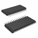 9DB106BGILFT

The activity of extra discounts on wholesale prices is in full swing…
Please fill in your contact information and we will send you the latest wholesale price list.







