 ChipApex | Global Electronic Components Supplier
9DB1200CGLFT
Search Product
Search Post
— IC芯片 | 连接器 | 传感器 | 被动器件 —
Search productSearch post
— IC芯片 | 连接器 | 传感器 | 被动器件 —
Consult the customer manager about the wholesale price.
consultation hotline:86-132-6715-2157
email:[email protected]
Contact the product manager for consultation. One-stop consultation is available.
Do you want a lower wholesale price? Please send us your inquiry and we will reply immediately.
The 9DB1200CGLFT is a PCI Express clock buffer and driver manufactured by Renesas Electronics Corporation. It features a single input to twelve output configuration with a maximum frequency of 400MHz. The device operates on a supply voltage ranging from 3.135V to 3.465V and supports both differential input and output signals. It utilizes HCSL output logic and includes an integrated PLL for jitter attenuation. The component is housed in a 64-TFSOP package, measuring 6.10mm in width, and is designed for surface mount installation within an operating temperature range of 0°C to 70°C.
Verify the current lifecycle status as the component is listed as discontinued. Confirm availability through authorized distributors or surplus channels. Ensure compliance with RoHS3 specifications and check for specific packaging options such as tape and reel or cut tape. Validate that the 64-TFSOP footprint matches the target PCB design requirements before procurement.
Select this component when a 1:12 fan-out solution is required for PCIe applications up to 400MHz. Ensure the design accommodates the 3.135V to 3.465V supply voltage range. Verify that the HCSL output compatibility aligns with downstream receiver inputs. Consider the 64-pin TSSOP package constraints for thermal management and board space allocation during the schematic capture phase.
This part belongs to the 9DB1200 series of clock buffers. It serves as a specialized timing solution for high-speed serial interfaces like PCI Express. The device integrates buffering and multiplexing capabilities to maintain signal integrity across multiple loads. It is distinct from other series members by its specific 1:12 output count and 400MHz frequency capability.
Renesas recommends RC19013A100GNG#KB0 as a manufacturer-recommended alternative. Verify pinout compatibility and electrical parameter alignment before substitution.
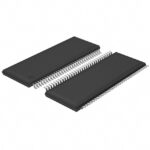 9DB1200CGLFT
The activity of extra discounts on wholesale prices is in full swing…
Please fill in your contact information and we will send you the latest wholesale price list.






