 ChipApex | Global Electronic Components Supplier
9DB833AGILF
Search Product
Search Post
— IC芯片 | 连接器 | 传感器 | 被动器件 —
Search productSearch post
— IC芯片 | 连接器 | 传感器 | 被动器件 —
Consult the customer manager about the wholesale price.
consultation hotline:86-132-6715-2157
email:[email protected]
Contact the product manager for consultation. One-stop consultation is available.
Do you want a lower wholesale price? Please send us your inquiry and we will reply immediately.
The Renesas 9DB833AGILF is an eight-output PCIe Gen1/Gen2/Gen3 zero-delay buffer and fanout clock distribution IC. It operates with a supply voltage range of 3.135 V to 3.465 V and supports maximum input frequencies up to 166 MHz. The device features differential HCSL inputs and outputs, providing low phase jitter performance compliant with PCIe Gen3 specifications (<1 ps RMS). Packaged in a 48-pin TSSOP, it supports both zero-delay buffer mode for precise timing alignment and fanout mode for signal distribution.
Verify the specific suffix 'GILF' against official Renesas documentation to confirm package type (TSSOP-48), lead-free status, and RoHS compliance. Confirm that the 'I' designation corresponds to the industrial temperature range (-40°C to +85°C) as distinct from commercial variants. Ensure sourcing channels provide valid traceability for this active component.
Select the 9DB833AGILF when designing systems requiring eight buffered PCIe clock outputs with strict jitter requirements for Gen3 speeds. Compare against the 9DB833AFLFT if a different package or temperature rating is needed, noting that the latter may be obsolete. Ensure the design accommodates the 3.3V supply requirement and differential HCSL signaling levels.
This component belongs to the 9DB833 family of zero-delay buffers designed specifically for high-speed serial interface applications. It serves as a critical timing element in complex digital systems, replacing older buffering solutions by integrating PLL functionality and multiple outputs into a single compact surface-mount package.
The 9DB833AFLFT is listed as a similar replacement option, though availability and exact parameter matching should be verified. Other family members like the 9DB233AGLFT (2 outputs) or 9DB433AGILFT (4 outputs) offer fewer channels but share similar electrical characteristics.
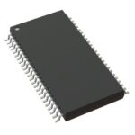 9DB833AGILF
The activity of extra discounts on wholesale prices is in full swing…
Please fill in your contact information and we will send you the latest wholesale price list.





