 ChipApex | Global Electronic Components Supplier
9DBL0442BKILF
Search Product
Search Post
— IC芯片 | 连接器 | 传感器 | 被动器件 —
Search productSearch post
— IC芯片 | 连接器 | 传感器 | 被动器件 —
Consult the customer manager about the wholesale price.
consultation hotline:86-132-6715-2157
email:[email protected]
Contact the product manager for consultation. One-stop consultation is available.
Do you want a lower wholesale price? Please send us your inquiry and we will reply immediately.
The Renesas 9DBL0442BKILF is a 3.3V PCIe clock buffer featuring four low-power HCSL (LP-HCSL) outputs with integrated 100Ω termination resistors. Designed for PCIe Gen1 through Gen5 architectures, it supports Common Clock (CC), Separate Reference Independent Spread (SRIS), and Separate Reference No Spread (SRNS) modes. The device operates within a frequency range of 1MHz to 200MHz in fanout mode and includes dedicated output enable pins for each channel.
Verify the suffix 'B' against official documentation to confirm specific manufacturing lot or revision details, as standard listings often reference the 'C' variant. Confirm moisture sensitivity level handling requirements prior to assembly. Ensure compatibility with the target PCB footprint for the 32-VFQFPN package.
Select this component when 100Ω transmission line termination is required directly at the source. Compare jitter performance specifications against the 9DBL0452 series if 85Ω termination is preferred. Verify that the 1MHz–200MHz operating range meets the system's clock frequency requirements.
This part belongs to the Renesas 9DBL0x family of low-power PCIe clock buffers. These devices are engineered to reduce board space by eliminating external termination resistors. The family supports various output counts and termination values to accommodate different PCIe topology requirements.
The 9DBL0442CKILF serves as a direct functional substitute within the same product family, differing primarily in the ordering suffix which may indicate packaging or revision variations.
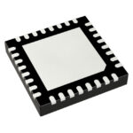 9DBL0442BKILF
The activity of extra discounts on wholesale prices is in full swing…
Please fill in your contact information and we will send you the latest wholesale price list.






