 ChipApex | Global Electronic Components Supplier
9DBL0442CKILFT
Search Product
Search Post
— IC芯片 | 连接器 | 传感器 | 被动器件 —
Search productSearch post
— IC芯片 | 连接器 | 传感器 | 被动器件 —
Consult the customer manager about the wholesale price.
consultation hotline:86-132-6715-2157
email:[email protected]
Contact the product manager for consultation. One-stop consultation is available.
Do you want a lower wholesale price? Please send us your inquiry and we will reply immediately.
The Renesas 9DBL0442CKILFT is a four-output PCIe clock buffer operating at 3.3V with integrated 100Ω termination resistors. It supports Low Power HCSL (LP-HCSL) signaling for PCIe Gen1 through Gen5 architectures, including Common Clock (CC), Separate Reference Independent Spread (SRIS), and Separate Reference No Spread (SRNS). The device functions in fan-out mode from 1MHz to 200MHz. Key electrical parameters include a supply voltage range of 3.135V to 3.465V, a maximum input frequency of 125MHz, and an operating temperature range of -40°C to +85°C.
Verify RoHS compliance status and moisture sensitivity level (MSL) ratings prior to procurement. Confirm the specific suffix 'CKILFT' corresponds to the required tape-and-reel packaging quantity and lead finish specifications. Ensure the component meets the intended thermal management requirements for the -40°C to +85°C industrial operating range.
Select this model when 100Ω transmission line termination is required directly on-chip, eliminating external resistors. Choose over the 9DBL0445 variant if the design utilizes 100Ω lines rather than 85Ω. Ensure the system clock frequency falls within the 1MHz to 200MHz fan-out range and that the 3.3V supply voltage remains within the specified 3.135V to 3.465V limits.
This component belongs to the Renesas 9DBL0x family of low-power, high-performance PCIe clock buffers. The family provides scalable output counts from two to eight channels across various package types. The 9DBL0442C specifically denotes the four-channel variant with 100Ω integrated termination, designed to reduce board space and simplify PCB layout for high-speed serial interfaces.
Publicly confirmed substitute part numbers are not available in the provided documentation. Verify pin-to-pin compatibility and electrical parameter alignment before considering alternative vendors or different series components.
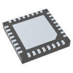 9DBL0442CKILFT
The activity of extra discounts on wholesale prices is in full swing…
Please fill in your contact information and we will send you the latest wholesale price list.





