 ChipApex | Global Electronic Components Supplier
9DBL0453ANLGI8
Search Product
Search Post
— IC芯片 | 连接器 | 传感器 | 被动器件 —
Search productSearch post
— IC芯片 | 连接器 | 传感器 | 被动器件 —
Consult the customer manager about the wholesale price.
consultation hotline:86-132-6715-2157
email:[email protected]
Contact the product manager for consultation. One-stop consultation is available.
Do you want a lower wholesale price? Please send us your inquiry and we will reply immediately.
The 9DBL0453ANLGI8 is a four-output, 3.3V PCIe zero-delay/fanout clock buffer from Renesas Electronics Corporation. It supports PCIe Gen 1 through Gen 6 and accommodates both Common Clock (CC) and Independent Reference (IR) architectures. The device features low-power HCSL (LP-HCSL) outputs that eliminate the need for external termination resistors on each output pair. It operates within a frequency range of 1 MHz to 200 MHz in fanout mode and accepts spread spectrum inputs. Configuration is managed via pin strapping or an SMBus interface with three selectable addresses.
Verify component authenticity through authorized Renesas distributors. Confirm RoHS3 compliance and MSL ratings against current datasheets. Check for PCN notifications regarding assembly site changes or marking updates. Ensure compatibility with system voltage requirements and thermal constraints before integration.
Select this buffer for designs requiring low-jitter distribution of PCIe reference clocks. The integrated termination simplifies PCB layout by removing external resistors. Verify that the required number of outputs matches the four available channels. Consider SMBus configuration needs if dynamic reprogramming is necessary during operation.
This component belongs to Renesas' comprehensive family of PCIe clocking solutions. It complements other devices like the 9DBL02x and 9DML series by providing specific zero-delay buffering capabilities. The product line targets high-speed serial communication standards, ensuring signal integrity across various generations of PCI Express interfaces.
Direct substitutes include the 9DBL0452NLGI8. Verify pinout compatibility and electrical specifications before substitution. Alternative models may offer different output counts or termination options.
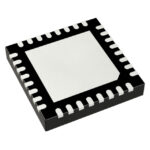 9DBL0453ANLGI8
The activity of extra discounts on wholesale prices is in full swing…
Please fill in your contact information and we will send you the latest wholesale price list.






