 ChipApex | Global Electronic Components Supplier
9DBL0455PGGI
Search Product
Search Post
— IC芯片 | 连接器 | 传感器 | 被动器件 —
Search productSearch post
— IC芯片 | 连接器 | 传感器 | 被动器件 —
Consult the customer manager about the wholesale price.
consultation hotline:86-132-6715-2157
email:[email protected]
Contact the product manager for consultation. One-stop consultation is available.
Do you want a lower wholesale price? Please send us your inquiry and we will reply immediately.
The 9DBL0455PGGI is a 4-output PCIe clock fanout buffer supporting Gen1 through Gen7. It operates on a 3.3V supply with LP-HCSL outputs and accepts HCSL inputs. The device features additive phase jitter of 300fs RMS typical, supports spread spectrum inputs, and includes SMBus configuration. It is housed in a 20-TSSOP package.
Verify the specific suffix PGGI against official Renesas documentation to confirm pin compatibility and package type. Ensure the procurement channel provides valid RoHS compliance data. Confirm that the active status aligns with current production schedules. Request detailed datasheets for accurate electrical parameter validation before integration into design specifications.
Select this component when designing systems requiring PCIe Gen1 through Gen7 clock buffering. It is suitable for architectures needing four differential outputs from a single source. Consider its 3.3V operation and LP-HCSL output signaling for compatibility with standard PCIe receiver inputs. Evaluate SMBus configuration needs if dynamic adjustment is required.
This part belongs to the 9DBL04xx family of PCIe clock buffers from Renesas. It complements other variants like the 9DBL0452 by offering specific output configurations and packaging options. The family targets high-speed serial link applications requiring precise timing and low jitter performance across multiple PCIe generations.
Check the 9DBL0452 datasheet for potential functional overlap. Verify pin-to-pin compatibility and electrical parameters before substitution. Ensure the alternative part supports the same PCIe generation requirements and output signaling standards.
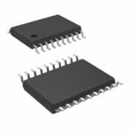 9DBL0455PGGI
The activity of extra discounts on wholesale prices is in full swing…
Please fill in your contact information and we will send you the latest wholesale price list.





