 ChipApex | Global Electronic Components Supplier
9DBU0641AKLF
Search Product
Search Post
— IC芯片 | 连接器 | 传感器 | 被动器件 —
Search productSearch post
— IC芯片 | 连接器 | 传感器 | 被动器件 —
Consult the customer manager about the wholesale price.
consultation hotline:86-132-6715-2157
email:[email protected]
Contact the product manager for consultation. One-stop consultation is available.
Do you want a lower wholesale price? Please send us your inquiry and we will reply immediately.
The Renesas 9DBU0641AKLF is a PCIe zero-delay fanout buffer designed for high-speed digital interfaces. It accepts an HCSL differential input and provides six LP-HCSL differential outputs. The device operates on a single 1.5V supply voltage, with a specified range of 1.425V to 1.575V. It supports maximum output frequencies up to 167MHz, suitable for PCIe Gen1 through Gen3 applications. The component is housed in a 40-pin VFQFPN package with exposed pad, measuring 5x5mm, and functions within a temperature range of -40°C to +85°C.
Verify the specific suffix 'AKLF' against the official datasheet to confirm package type and temperature grade. Confirm RoHS compliance status via the manufacturer's latest documentation. Check for moisture sensitivity level requirements during storage and handling. Ensure the ordering quantity matches the standard factory packaging specifications provided by Renesas.
Select this component when a single HCSL clock source needs to drive multiple PCIe endpoints with zero skew. Compare against the 9DBU0631 series if fewer than six outputs are required. Verify that the system power budget accommodates the 1.5V rail and the specific current draw of the LP-HCSL outputs. Ensure the PCB layout supports the 40-VFQFPN footprint for optimal thermal performance.
This part belongs to the 9DBU06xx family of PCIe clock buffers from Renesas. It serves as a distribution solution for high-speed serial links where signal integrity and timing precision are critical. It complements clock generators like the 9FGV series by providing buffered outputs for downstream logic.
The 9DBU0631AKILF is a related variant within the same family. Verify pin compatibility and electrical parameters before substitution. No direct cross-manufacturer equivalents are listed in public documentation without further validation.
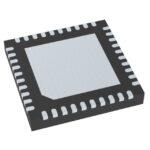 9DBU0641AKLF
The activity of extra discounts on wholesale prices is in full swing…
Please fill in your contact information and we will send you the latest wholesale price list.







