ChipApex | Global Electronic Components Supplier
9DBU0831AKLFT
Search Product
Search Post
— IC芯片 | 连接器 | 传感器 | 被动器件 —
Search productSearch post
— IC芯片 | 连接器 | 传感器 | 被动器件 —
Consult the customer manager about the wholesale price.
consultation hotline:86-132-6715-2157
email:[email protected]
Contact the product manager for consultation. One-stop consultation is available.
Do you want a lower wholesale price? Please send us your inquiry and we will reply immediately.
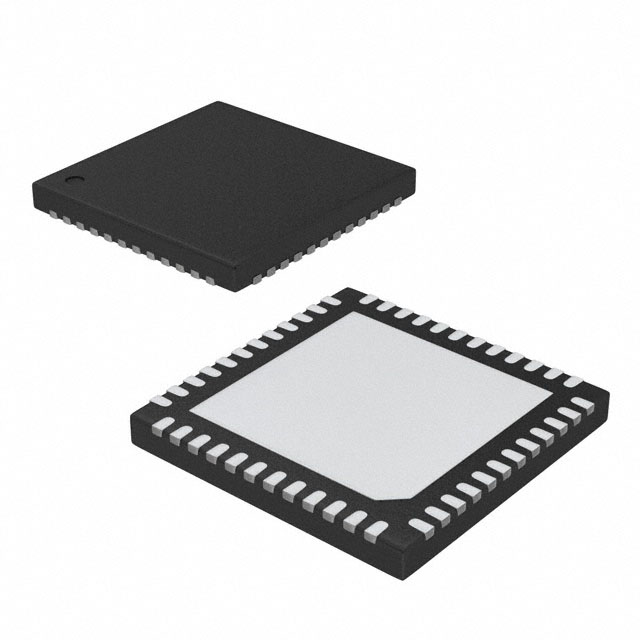
The Renesas 9DBU0831AKLFT is an 8-output low-power clock buffer designed for PCIe Gen 1/2/3 and QPI/UPI applications. It features a single HCSL-compatible differential input and eight LP-HCSL differential outputs, operating within a frequency range of 33 MHz to 150 MHz. The device requires a 3.3 V supply voltage and consumes approximately 445 mW of typical power. Packaged in a space-saving 48-pin VFQFPN (6x6 mm) format, it supports spread spectrum inputs and includes hardware control via eight output enable pins.
Verify the suffix 'AKLFT' confirms the specific tape-and-reel packaging and lead-free composition. Confirm moisture sensitivity level (MSL) ratings and reflow soldering profiles against current datasheet revisions before procurement planning.
Select this component when interfacing with PCIe or QPI/UPI sources requiring low-power distribution. Ensure the design accommodates the 3.3 V supply requirement and the 48-pin VFQFPN footprint. Compare against the 9ZXL0831 series if lower power consumption is critical, noting the trade-off in performance specifications.
This part belongs to the IDT/Renesas ultra-low-power PCIe clock buffer family. It serves as a fanout buffer to distribute reference clocks to multiple downstream components while maintaining signal integrity and minimizing power dissipation in high-density electronic systems.
The 9ZXL0831E is noted as a pin-to-pin alternative with improved performance and reduced external components. Verify electrical compatibility and package dimensions before substitution.
 9DBU0831AKLFT
The activity of extra discounts on wholesale prices is in full swing…
Please fill in your contact information and we will send you the latest wholesale price list.