ChipApex | Global Electronic Components Supplier
9DBU0941AKILFT
Search Product
Search Post
— IC芯片 | 连接器 | 传感器 | 被动器件 —
Search productSearch post
— IC芯片 | 连接器 | 传感器 | 被动器件 —
Consult the customer manager about the wholesale price.
consultation hotline:86-132-6715-2157
email:[email protected]
Contact the product manager for consultation. One-stop consultation is available.
Do you want a lower wholesale price? Please send us your inquiry and we will reply immediately.
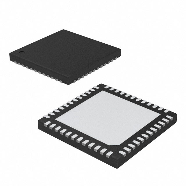
The 9DBU0941AKILFT is a PCIe fanout clock buffer manufactured by Renesas Electronics Corporation. It features a single circuit with a 1:9 input-to-output ratio, supporting differential HCSL and LVDS inputs alongside LP-HCSL outputs. The device operates at a maximum frequency of 167MHz within a supply voltage range of 1.425V to 1.575V. Designed for surface mount installation, it is housed in a 48-VFQFPN package with exposed pads (6x6mm). The component functions without an internal PLL and supports operation across a temperature range of 0°C to 70°C.
Verify the specific suffix 'ILFT' against official Renesas documentation to confirm lead-free status and tape-and-reel packaging specifications. Confirm current product lifecycle status, as timing components frequently undergo obsolescence notices or manufacturing site changes that may affect long-term availability.
Select this component when a single reference clock must drive nine distinct PCIe endpoints requiring LP-HCSL outputs. Ensure the design accommodates the 1.5V nominal supply voltage and verify that the board layout supports the 48-pin VFQFPN footprint with adequate thermal relief for the exposed pad.
This part belongs to the 9DBU series of PCIe clock buffers from Renesas. It serves as a specialized distribution element for high-speed serial interfaces, differing from general-purpose clock generators by focusing on low-jitter fanout capabilities tailored for PCI Express compliance requirements.
Consult the official Renesas cross-reference guide for verified pin-compatible alternatives. Generic clock buffers may not support the specific HCSL/LVDS input flexibility or LP-HCSL output characteristics required for PCIe Gen1-Gen3 compatibility.
 9DBU0941AKILFT
The activity of extra discounts on wholesale prices is in full swing…
Please fill in your contact information and we will send you the latest wholesale price list.