 ChipApex | Global Electronic Components Supplier
9DBU0941AKLF
Search Product
Search Post
— IC芯片 | 连接器 | 传感器 | 被动器件 —
Search productSearch post
— IC芯片 | 连接器 | 传感器 | 被动器件 —
Consult the customer manager about the wholesale price.
consultation hotline:86-132-6715-2157
email:[email protected]
Contact the product manager for consultation. One-stop consultation is available.
Do you want a lower wholesale price? Please send us your inquiry and we will reply immediately.
The 9DBU0941AKLF is a PCIe fanout clock buffer manufactured by Renesas Electronics Corporation. It features a single input to nine differential output configuration with a maximum frequency of 167MHz. The device operates on a 1.5V supply voltage (1.425V to 1.575V) and utilizes HCSL input and LP-HCSL output signaling standards. Packaged in a 48-VFQFPN (6x6mm) surface-mount housing, it supports both common clocked and separate reference architectures for PCI Express Gen1 through Gen3 applications.
Verify component authenticity through authorized channels due to potential counterfeit risks. Confirm RoHS compliance status as the product may be subject to end-of-life notices or manufacturing transitions. Check specific ordering suffixes for package variations such as tape-and-reel versus tray packaging before procurement.
Select this component when nine differential clock outputs are required for PCIe expansion slots or peripherals. Ensure the design accommodates the 1.5V supply rail and HCSL/LP-HCSL interface requirements. Verify that the 48-pin VFQFPN package footprint aligns with the PCB layout constraints and thermal management capabilities of the target application.
This part belongs to the Renesas 9DBU series of PCIe clock buffers. It is designed to replace legacy discrete clocking solutions by integrating multiple outputs and termination resistors into a single compact package, thereby reducing board space and component count in high-density server designs.
Direct pin-to-pin replacements within the same family include the 9DBU0941AKILF, which offers an extended industrial temperature range (-40°C to 85°C). Other members of the 9DBV0941 family may serve as functional alternatives if voltage levels and packaging formats are compatible.
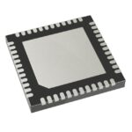 9DBU0941AKLF
The activity of extra discounts on wholesale prices is in full swing…
Please fill in your contact information and we will send you the latest wholesale price list.






