 ChipApex | Global Electronic Components Supplier
9DBV0231AKILF
Search Product
Search Post
— IC芯片 | 连接器 | 传感器 | 被动器件 —
Search productSearch post
— IC芯片 | 连接器 | 传感器 | 被动器件 —
Consult the customer manager about the wholesale price.
consultation hotline:86-132-6715-2157
email:[email protected]
Contact the product manager for consultation. One-stop consultation is available.
Do you want a lower wholesale price? Please send us your inquiry and we will reply immediately.
The 9DBV0231AKILF is a low-power, 2-output PCIe zero-delay/fanout clock buffer manufactured by Renesas Electronics. Operating at a core voltage of 1.8V, it features LP-HCSL differential outputs and an HCSL-compatible differential input. The device supports output frequencies from 30 MHz to 137.5 MHz with typical power consumption of 35 mW in PLL mode. It is housed in a space-saving 24-pin VFQFPN package (4.0 x 4.0 mm). Key capabilities include spread spectrum compatibility, programmable slew rate and amplitude, and SMBus-selectable features for signal integrity optimization.
Verify the specific suffix 'AKILF' against the official datasheet to confirm package dimensions and moisture sensitivity level. Ensure the ordering quantity aligns with the manufacturer's reel or tray specifications. Confirm RoHS compliance status through the latest product change notifications before procurement.
Select this component when a 1.8V supply is available and LP-HCSL signaling is required to minimize power and board area. Compare against the 9DBU0231 if a 1.5V core voltage is necessary for the application. Verify that the 137.5 MHz maximum frequency meets the target bus speed requirements.
This part belongs to the IDT/Renesas 9DBV0231 family of ultra-low-power PCIe clock buffers. It serves as a fanout buffer and zero-delay buffer for high-speed serial links. The device integrates configuration options via strapping pins or SMBus, allowing flexibility in slew rate and amplitude tuning without external components.
The 9DBU0231 is a similar 2-output buffer but operates at 1.5V instead of 1.8V. The 9DBV0431 offers 4 outputs in a different package. Verify pin compatibility and voltage levels before substituting.
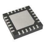 9DBV0231AKILF
The activity of extra discounts on wholesale prices is in full swing…
Please fill in your contact information and we will send you the latest wholesale price list.







