 ChipApex | Global Electronic Components Supplier
9DBV0631BKILF
Search Product
Search Post
— IC芯片 | 连接器 | 传感器 | 被动器件 —
Search productSearch post
— IC芯片 | 连接器 | 传感器 | 被动器件 —
Consult the customer manager about the wholesale price.
consultation hotline:86-132-6715-2157
email:[email protected]
Contact the product manager for consultation. One-stop consultation is available.
Do you want a lower wholesale price? Please send us your inquiry and we will reply immediately.
The 9DBV0631BKILF is a six-output, 1.8V PCIe zero-delay/fanout clock buffer manufactured by Renesas Electronics Corporation. It belongs to the Ultra-Low-Power (ULP) PCIe family and features LP-HCSL differential outputs. The device supports spread spectrum input for EMI reduction and includes three selectable SMBus addresses for configuration. It operates with a supply voltage range of 1.05V to 1.5V or 1.5V to 1.5V, consuming approximately 47mW typically in PLL mode. The component is housed in a 40-lead VFQFPN package measuring 5.0mm x 5.0mm with a 0.4mm pitch.
Verify the specific suffix BKILF against official Renesas documentation to confirm package type and tape-and-reel specifications. Ensure compatibility with 1.8V PCIe standards and check for any lead-free or RoHS compliance certifications required for your manufacturing process. Confirm availability status as this component may be subject to lifecycle changes.
Select this component when designing systems requiring multiple low-power differential clock outputs from a single source. It is suitable for applications needing spread spectrum capability to meet strict EMI regulations. Consider the VFQFPN package size for space-constrained PCB layouts. Verify that the host controller supports the required SMBus interface for configuring the selectable addresses and output enables.
This part is part of Renesas' IDT portfolio of PCIe clock buffers, designed to replace legacy clock generators with lower power consumption solutions. It integrates functions previously handled by separate components, such as termination resistors and level shifters, into a single compact package. The device is engineered to support the evolving requirements of high-speed serial interfaces like PCIe.
Consult official substitution guides for pin-compatible alternatives within the 9DBV series. Verify electrical parameters such as output frequency range and power consumption before replacing. Ensure the replacement part supports the same 1.8V supply and LP-HCSL output signaling.
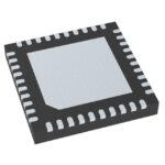 9DBV0631BKILF
The activity of extra discounts on wholesale prices is in full swing…
Please fill in your contact information and we will send you the latest wholesale price list.





