 ChipApex | Global Electronic Components Supplier
9DBV0631BKLF
Search Product
Search Post
— IC芯片 | 连接器 | 传感器 | 被动器件 —
Search productSearch post
— IC芯片 | 连接器 | 传感器 | 被动器件 —
Consult the customer manager about the wholesale price.
consultation hotline:86-132-6715-2157
email:[email protected]
Contact the product manager for consultation. One-stop consultation is available.
Do you want a lower wholesale price? Please send us your inquiry and we will reply immediately.
The 9DBV0631BKLF is a six-output, 1.8 V PCIe zero-delay clock buffer manufactured by Renesas Electronics Corporation. It belongs to the 9DBV05x1-9DBV07x1 family and supports PCIe Gen1 through Gen3 standards. The device features integrated terminations for direct connection to 100 Ω transmission lines and includes six output enable pins for flexible clock management. It offers three selectable SMBus addresses for configuration control. The component is housed in a 48-lead VFQFPN package with dimensions of 6.0 x 6.0 x 0.9 mm and operates within a commercial temperature range of 0°C to 70°C.
The 9DBV0631BKLF is classified as obsolete or end-of-life by the manufacturer. Verification of current availability requires checking authorized distributors directly, as stock levels are not guaranteed. Designers should confirm lead times and potential obsolescence risks before finalizing procurement plans for this specific part number.
Select the 9DBV0631BKLF when a six-channel 1.8 V PCIe clock buffer with zero-delay feedback is required. Ensure the design utilizes the 48-lead VFQFPN footprint (6.0 x 6.0 mm). Verify that the system voltage matches the 1.8 V specification and that SMBus compatibility aligns with the controller's address settings.
This component is part of the broader 9DBV series from Renesas, which includes variants with different output counts such as the 9DBV05x1, 9DBV07x1, and 9DBV09x1 families. These devices share similar architectural features tailored for PCIe clock generation and distribution, differing primarily in the number of outputs and specific package configurations.
Direct replacements may include other members of the 9DBV family, such as the 9DBV0531 or 9DBV0731, depending on whether fewer or additional outputs are acceptable. Cross-referencing pinouts and electrical specifications with the official datasheet is essential to ensure functional compatibility.
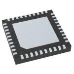 9DBV0631BKLF
The activity of extra discounts on wholesale prices is in full swing…
Please fill in your contact information and we will send you the latest wholesale price list.






