 ChipApex | Global Electronic Components Supplier
9DBV0841AKLFT
Search Product
Search Post
— IC芯片 | 连接器 | 传感器 | 被动器件 —
Search productSearch post
— IC芯片 | 连接器 | 传感器 | 被动器件 —
Consult the customer manager about the wholesale price.
consultation hotline:86-132-6715-2157
email:[email protected]
Contact the product manager for consultation. One-stop consultation is available.
Do you want a lower wholesale price? Please send us your inquiry and we will reply immediately.
The 9DBV0841AKLFT is an 8-output, 1.8V PCIe fanout clock buffer manufactured by Renesas Electronics Corporation. It features a single differential HCSL input and eight low-power HCSL (LP-HCSL) differential outputs. The device supports operating frequencies from 1 MHz to 200 MHz and includes integrated 100Ω terminations for direct connection to transmission lines. Key specifications include a typical power consumption of 50 mW, support for spread spectrum modulation, and selectable SMBus addresses for configuration management. It is housed in a space-saving 32-pin VFQFPN package measuring 5.0 mm x 5.0 mm.
Verify component authenticity through authorized distributors as counterfeit risks exist for high-volume clocking ICs. Confirm RoHS3 compliance and lead-free status (Pb Free Category e3 Sn). Check Moisture Sensitivity Level (MSL 3) handling requirements during storage and assembly. Ensure the specific suffix matches the required temperature grade and packaging format.
Select this component when designing for PCIe Gen1 through Gen5 environments requiring low-voltage 1.8V signaling. The integrated 100Ω termination eliminates external resistors, saving board space compared to standard HCSL buffers. Verify that the input source provides a compatible HCSL signal and that the system requires spread spectrum tolerance for EMI reduction.
This part belongs to the 9DBV05x1-07x1-09x1 family of PCIe fanout clock buffers. It shares architectural similarities with the 9DBV0541 (5-output) and 9DBV0941 (9-output) variants, differing primarily in output count and pin configuration. The device is designed to replace discrete resistor networks in high-speed digital designs.
Direct functional substitutes within the same family include the 9DBV0541 (5 outputs) or 9DBV0941 (9 outputs), provided the output count difference is acceptable. Cross-family replacements require verification of voltage levels (1.8V vs 3.3V) and package compatibility.
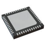 9DBV0841AKLFT
The activity of extra discounts on wholesale prices is in full swing…
Please fill in your contact information and we will send you the latest wholesale price list.





