 ChipApex | Global Electronic Components Supplier
9FGL08P1A000KILFT
Search Product
Search Post
— IC芯片 | 连接器 | 传感器 | 被动器件 —
Search productSearch post
— IC芯片 | 连接器 | 传感器 | 被动器件 —
Consult the customer manager about the wholesale price.
consultation hotline:86-132-6715-2157
email:[email protected]
Contact the product manager for consultation. One-stop consultation is available.
Do you want a lower wholesale price? Please send us your inquiry and we will reply immediately.
The 9FGL08P1A000KILFT is an eight-output PCIe clock generator from Renesas Electronics, designed for high-performance computing and server applications. It supports PCIe Gen 1 through Gen 6 architectures, including Common Clocked (CC), Separate Reference no Spread (SRNS), and Separate Reference Independent Spread (SRIS). The device operates at a nominal 3.3V supply voltage with a range of 3.135V to 3.465V. It features integrated terminations for both 100Ω and 85Ω systems, reducing external component count. The unit is housed in a compact 48-lead VFQFPN package and functions within a temperature range of -40°C to +85°C.
Verify the specific suffix 'A000' against official Renesas documentation to confirm pinout and configuration settings, as suffixes often denote factory-programmed SMBus defaults or specific hardware strapping options. Ensure the 48-VFQFPN package dimensions align with PCB layout requirements. Confirm moisture sensitivity level (MSL) handling procedures during assembly.
Select this component when designing PCIe Gen 1–6 interfaces requiring eight synchronized clock outputs. It is suitable for systems needing integrated termination resistors to save board space. Consider the 9FGL0851D variant if only six outputs are required or if different spread spectrum configurations are preferred. Verify input frequency compatibility (typically 25MHz or 100MHz crystal/LVCMOS) before integration.
This part belongs to the 9FGL08xx series of PCIe clock generators. It shares architectural similarities with the 9FGL0241/51 and 9FGL0441/51 devices but provides eight outputs instead of two or four. It is part of Renesas' broader portfolio of low-power clock solutions for data communication and storage applications.
Direct substitutes include other members of the 9FGL08xx family, such as the 9FGL0851D, provided the output count and electrical specifications match the design requirements. Cross-referencing with the 9FGL0831CKILF is possible for legacy PCIe Gen 1–3 designs, though voltage levels and feature sets differ.
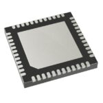 9FGL08P1A000KILFT
The activity of extra discounts on wholesale prices is in full swing…
Please fill in your contact information and we will send you the latest wholesale price list.






