ChipApex | Global Electronic Components Supplier
9FGV0631CKILF
Search Product
Search Post
— IC芯片 | 连接器 | 传感器 | 被动器件 —
Search productSearch post
— IC芯片 | 连接器 | 传感器 | 被动器件 —
Consult the customer manager about the wholesale price.
consultation hotline:86-132-6715-2157
email:[email protected]
Contact the product manager for consultation. One-stop consultation is available.
Do you want a lower wholesale price? Please send us your inquiry and we will reply immediately.
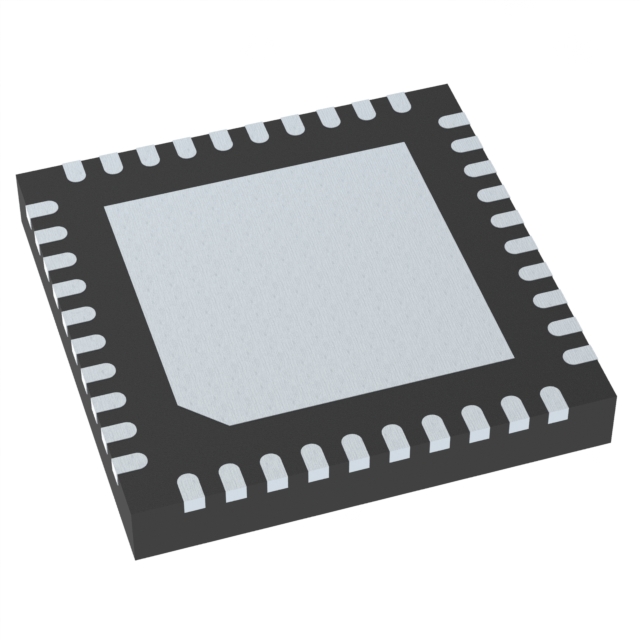
The Renesas 9FGV0631CKILF is a PCI Express clock generator featuring one circuit with a 1:6 input-to-output ratio. It accepts LVDS or crystal inputs and provides LP-HCSL and LVCMOS outputs. The device supports a maximum frequency of 100 MHz and operates on a 1.7 V to 1.9 V supply voltage. Housed in a 40-VFQFPN (5x5) package, it functions within an ambient temperature range of -40°C to 85°C.
Verify the specific suffix CKILF against official documentation to confirm package dimensions and moisture sensitivity level. Confirm RoHS compliance status through manufacturer datasheets prior to procurement. Ensure availability aligns with current production lifecycle status.
Select this component for applications requiring a single PLL circuit with six differential or single-ended outputs. Verify that the 1.7 V to 1.9 V supply range matches the system power rails. Ensure the 40-VFQFPN footprint fits the PCB layout constraints.
This part belongs to the Renesas 9FGV series of low-power PCIe clock generators. It is designed to replace legacy timing solutions by integrating PLL functionality and multiple output drivers into a compact surface-mount package suitable for high-density boards.
Consult official substitution guides for direct pin-compatible alternatives. Verify electrical parameters such as jitter performance and output drive strength when considering cross-family replacements.
 9FGV0631CKILF
The activity of extra discounts on wholesale prices is in full swing…
Please fill in your contact information and we will send you the latest wholesale price list.