ChipApex | Global Electronic Components Supplier
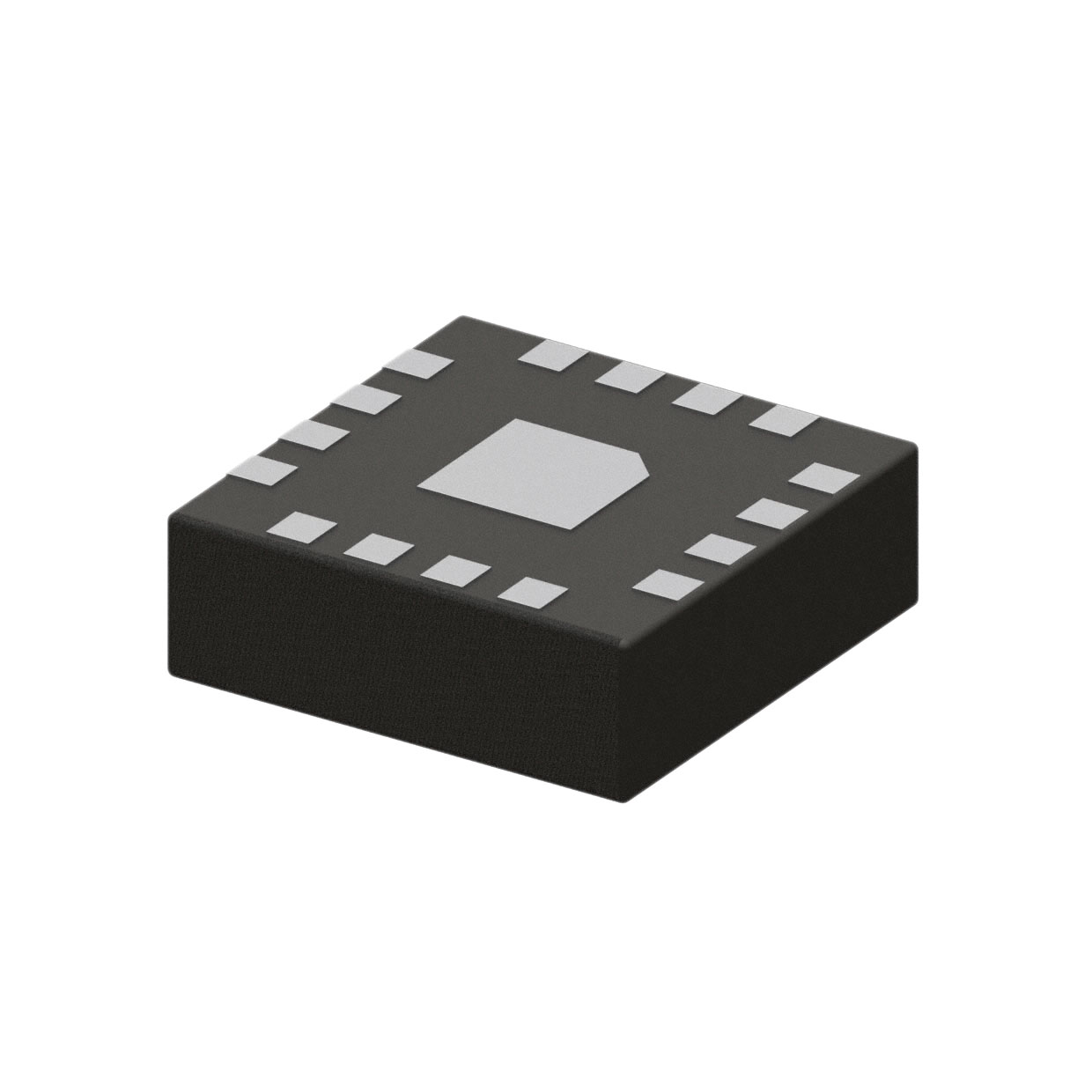
9FGV1001BQ508LTGI8
Search Product
Search Post
— IC芯片 | 连接器 | 传感器 | 被动器件 —
Search productSearch post
— IC芯片 | 连接器 | 传感器 | 被动器件 —
Consult the customer manager about the wholesale price.
consultation hotline:86-132-6715-2157
email:[email protected]
Contact the product manager for consultation. One-stop consultation is available.
Do you want a lower wholesale price? Please send us your inquiry and we will reply immediately.
The 9FGV1001BQ508LTGI8 is a programmable PhiClock generator from Renesas Electronics, designed for high-performance clock distribution. It features four differential LP-HCSL outputs and two crystal reference inputs. The device supports input frequencies of 50 MHz and provides output frequencies including 50 MHz, 100 MHz, 125 MHz, 156.25 MHz, 161.1328125 MHz, 312.5 MHz, and 322.265625 MHz. It operates on a single 1.8 V or 3.3 V supply with typical power consumption of 200 mW. The component is housed in a 24-lead LGA package (4.0 x 4.0 x 1.4 mm) and functions within a temperature range of -40°C to +85°C.
Verify the specific suffix LTGI8 indicates tape and reel packaging when ordering. Confirm the exact frequency configuration required, as this is a factory-programmable device. Check current availability status as lead times may vary. Ensure compatibility with existing PCB footprint for the 24-LGA package. Validate moisture sensitivity level handling procedures during assembly.
Select this model if four matched differential LP-HCSL outputs are required for symmetric clock distribution. Compare against other 9FGV1001 variants based on specific output frequency needs such as 100 MHz or 125 MHz. Consider the 1.8 V core voltage requirement for low-power designs. Evaluate the I²C configurability if dynamic frequency changes are needed versus fixed OTP configuration.
This part belongs to the Renesas PhiClock™ family of programmable clock generators. The 9FGV1001 series is optimized for meeting strict jitter budgets of modern high-speed interfaces like PCIe. It replaces discrete oscillator solutions by integrating PLL functionality and multiple output drivers into a single compact package.
Direct pin-to-pin replacements within the 9FGV1001 family depend on matching the output frequency and package type. Verify that alternative parts support the same LP-HCSL signaling and jitter specifications. Cross-reference with Renesas documentation for updated lifecycle status.
 9FGV1001BQ508LTGI8
The activity of extra discounts on wholesale prices is in full swing…
Please fill in your contact information and we will send you the latest wholesale price list.