 ChipApex | Global Electronic Components Supplier
9FGV1002C015NBGI8
Search Product
Search Post
— IC芯片 | 连接器 | 传感器 | 被动器件 —
Search productSearch post
— IC芯片 | 连接器 | 传感器 | 被动器件 —
Consult the customer manager about the wholesale price.
consultation hotline:86-132-6715-2157
email:[email protected]
Contact the product manager for consultation. One-stop consultation is available.
Do you want a lower wholesale price? Please send us your inquiry and we will reply immediately.
The Renesas 9FGV1002C015NBGI8 is a PhiClock programmable clock generator designed for Ethernet and PCI Express applications. It features an integrated PLL and supports input signals via HCSL, LVCMOS, LVDS, or crystal. The device provides one output with configurable signaling formats including CML, HCSL, LP-HCSL, LVCMOS, LVDS, and LVPECL. Operating voltage ranges are 1.71V to 1.89V, 2.375V to 2.625V, and 3.135V to 3.465V. Maximum frequencies are 200MHz and 325MHz. It operates within -40°C to 85°C and holds AEC-Q100 automotive qualification.
Verify the specific suffix NBGI8 against the official datasheet to confirm package type and tape/reel specifications. Ensure compatibility with system power supply rails of 1.8V, 2.5V, or 3.3V. Confirm that the factory-programmed configuration matches the design requirements, as this is a fixed-configuration variant.
Select this component when a single differential or single-ended output is required for PCIe or Ethernet interfaces. Compare against other PhiClock models based on the specific output voltage swing and load capacitance requirements. Verify that the 1:6 ratio capability aligns with the system's clock distribution needs.
This part belongs to the Renesas PhiClock family of programmable clock generators. The 9FGV1002 series is optimized for high-performance computing and communication applications requiring low jitter and flexible output configurations. It serves as a replacement for legacy clock buffer and generator ICs in modern serial link designs.
Check pin-to-pin compatibility with existing clock buffers if upgrading from older generations. Verify that the output drive strength and termination requirements match the PCB trace design. Ensure the I²C address settings do not conflict with other devices on the bus.
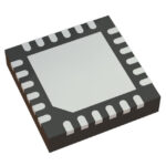 9FGV1002C015NBGI8
The activity of extra discounts on wholesale prices is in full swing…
Please fill in your contact information and we will send you the latest wholesale price list.





