 ChipApex | Global Electronic Components Supplier
9FGV1004B201NBGI8
Search Product
Search Post
— IC芯片 | 连接器 | 传感器 | 被动器件 —
Search productSearch post
— IC芯片 | 连接器 | 传感器 | 被动器件 —
Consult the customer manager about the wholesale price.
consultation hotline:86-132-6715-2157
email:[email protected]
Contact the product manager for consultation. One-stop consultation is available.
Do you want a lower wholesale price? Please send us your inquiry and we will reply immediately.
The Renesas 9FGV1004B201NBGI8 is a programmable PhiClock generator from the 9FGV1004 family, designed for low phase-noise and low-power applications. It supports PCIe Gen1 through Gen4 compliance with typical RMS phase jitter of 267fs at 156.25MHz (12kHz–20MHz). The device provides four programmable output pairs plus two LVCMOS reference outputs, supporting LP-HCSL, LVDS, and LVCMOS signaling standards. Operating frequencies range from 1MHz to 325MHz for integer outputs and up to 200MHz for LVCMOS. It features a 4x4 mm 24-VFQFPN package and includes an integrated crystal option.
Verify the specific suffix 'B201' against official Renesas documentation to confirm factory-configured frequency settings. Confirm package type matches the 24-VFQFPN variant. Check for any product change notifications affecting assembly locations or materials before procurement.
Select this component when PCIe Gen1-4 jitter specifications are required. Ensure the design supports LP-HCSL or LVDS differential signaling. Verify that the 1.8V or 3.3V core voltage aligns with system power rails. Consider I²C address availability if multiple clocks are used on the same bus.
This part belongs to the Renesas PhiClock™ programmable clock generator family. It offers flexible configuration via hardware pins or I²C software control. The device allows users to define default configurations in OTP memory for I²C mode operation.
Check for direct substitutes within the 9FGV1004 series with different output frequencies or packaging options. Verify compatibility with existing PCB footprints and signal integrity requirements when considering alternative packages.
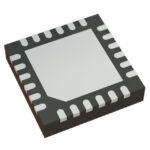 9FGV1004B201NBGI8
The activity of extra discounts on wholesale prices is in full swing…
Please fill in your contact information and we will send you the latest wholesale price list.





