 ChipApex | Global Electronic Components Supplier
9FGV1004B208NBGI
Search Product
Search Post
— IC芯片 | 连接器 | 传感器 | 被动器件 —
Search productSearch post
— IC芯片 | 连接器 | 传感器 | 被动器件 —
Consult the customer manager about the wholesale price.
consultation hotline:86-132-6715-2157
email:[email protected]
Contact the product manager for consultation. One-stop consultation is available.
Do you want a lower wholesale price? Please send us your inquiry and we will reply immediately.
The 9FGV1004B208NBGI is a programmable clock generator from Renesas Electronics' PhiClock family, designed for high-performance timing applications. It features four differential output pairs supporting LP-HCSL and LVDS signaling standards, with individual 1.8V to 3.3V VDDO control for each pair. The device operates within a supply voltage range of 1.71V to 3.465V and supports integer frequencies up to 325MHz. It utilizes a 24-pin VFQFPN package (4x4mm) and includes an integrated crystal option. Key specifications include a typical phase jitter of 267fs RMS at 156.25MHz and compliance with PCIe Gen1 through Gen4 standards.
Verify the specific suffix 'NBGI' against official Renesas documentation to confirm pinout and electrical characteristics, as suffixes often denote package type or temperature range. Confirm availability status, as some variants in this series may be discontinued or subject to long lead times. Ensure the selected part matches the required output frequency and voltage levels for the target application design.
Select this component when designing systems requiring four independent differential clock outputs with mixed voltage domains. The 9FGV1004B208NBGI is suitable for applications needing hardware-configurable default settings via select pins or software-controlled I²C access. Consider the 24-VFQFPN package constraints for PCB layout and thermal management. Verify that the input crystal frequency and desired output multiples align with the device's internal PLL capabilities.
This part belongs to the Renesas PhiClock 9FGV1004 series, which offers programmable clock generation solutions for high-speed digital interfaces. The series is characterized by its flexibility in output formats and low jitter performance, making it a common choice for modern computing and networking platforms. The NBGI suffix typically indicates a specific tape-and-reel or tray packaging variant for surface-mount assembly.
Direct replacements within the same family include other 9FGV1004 variants with different output configurations or voltage ranges. Cross-family alternatives from other manufacturers should be evaluated based on pin compatibility, jitter specifications, and supported output standards. Always verify that any substitute part meets the specific PCIe compliance requirements if used in such applications.
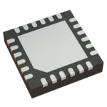 9FGV1004B208NBGI
The activity of extra discounts on wholesale prices is in full swing…
Please fill in your contact information and we will send you the latest wholesale price list.





