ChipApex | Global Electronic Components Supplier
9FGV1004BQ550LTGI8
Search Product
Search Post
— IC芯片 | 连接器 | 传感器 | 被动器件 —
Search productSearch post
— IC芯片 | 连接器 | 传感器 | 被动器件 —
Consult the customer manager about the wholesale price.
consultation hotline:86-132-6715-2157
email:[email protected]
Contact the product manager for consultation. One-stop consultation is available.
Do you want a lower wholesale price? Please send us your inquiry and we will reply immediately.
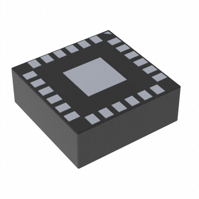
The Renesas 9FGV1004BQ550LTGI8 is a programmable clock generator from the PhiClock family, designed for high-performance timing applications. It features four differential output pairs supporting LP-HCSL and LVDS signaling standards. The device operates within a supply voltage range of 1.71 V to 3.465 V and supports maximum output frequencies up to 325 MHz. Packaged in a 24-lead VFQFPN format, it integrates spread-spectrum capabilities and offers jitter performance suitable for PCIe Gen1 through Gen4 compliance.
This component is classified as obsolete or end-of-life by the manufacturer. Availability is restricted to existing stock or surplus channels. Verification of authenticity and storage history is critical due to the discontinued status. Buyers should confirm the specific suffix LTGI8 indicates reel packaging and ensure compatibility with existing design implementations before procurement.
Select this part when four matched differential outputs are required for PCIe or similar high-speed serial links. Ensure the system design accommodates the 1.71 V to 3.465 V supply range and the 24-VFQFPN package footprint. Verify that the integrated crystal option or external reference input matches the system's clock source architecture. Consider the 27 ps jitter specification against the target application's noise budget.
The 9FGV1004 series belongs to Renesas' PhiClock programmable clock generator family, optimized for PCI Express and high-speed I/O applications. This specific model variant utilizes factory-programmed configurations accessible via I²C or hardware pins. It serves as a replacement for legacy fixed-frequency oscillators in multi-standard designs requiring flexible frequency synthesis.
Due to the obsolete status, direct replacements may be limited. Evaluate newer PhiClock variants such as the 9FGV1004C series for updated packaging or availability. Ensure any substitute maintains the same pinout, output signaling types (LP-HCSL/LVDS), and electrical characteristics to avoid redesign.
 9FGV1004BQ550LTGI8
The activity of extra discounts on wholesale prices is in full swing…
Please fill in your contact information and we will send you the latest wholesale price list.