 ChipApex | Global Electronic Components Supplier
9FGV1004CQ551LTGI8
Search Product
Search Post
— IC芯片 | 连接器 | 传感器 | 被动器件 —
Search productSearch post
— IC芯片 | 连接器 | 传感器 | 被动器件 —
Consult the customer manager about the wholesale price.
consultation hotline:86-132-6715-2157
email:[email protected]
Contact the product manager for consultation. One-stop consultation is available.
Do you want a lower wholesale price? Please send us your inquiry and we will reply immediately.
The Renesas 9FGV1004CQ551LTGI8 is a clock generator and jitter attenuator designed for high-performance digital systems. It features four output clocks with programmable frequencies, supporting LVDS and HCSL output types. The device integrates a phase-locked loop (PLL) for low-jitter performance and includes an I2C interface for configuration. Key specifications include a maximum input frequency of 200 MHz and output frequencies up to 600 MHz. It operates within a supply voltage range of 3.135 V to 3.465 V and is housed in a 48-pin QFN package.
Verify the specific ordering suffix LTGI8 confirms the tape-and-reel packaging and temperature grade. Confirm the exact frequency plan matches the application requirements as the device is programmable. Ensure compatibility with the system's I2C bus voltage levels and pull-up resistor values.
Select this component when multiple low-jitter outputs are required from a single source. Compare the available output formats (LVDS/HCSL) against the receiver inputs of the target devices. Verify that the input clock source meets the specified frequency range and signal integrity requirements for optimal PLL performance.
This part belongs to Renesas' 9FGV series of clock generators. It is designed to replace discrete oscillator solutions, reducing board space and power consumption. The 9FGV1004 variant specifically offers four outputs, making it suitable for complex multi-clock domains in modern electronic designs.
Direct replacements must match the 48-pin QFN package and pinout. Verify that alternative clock generators support the same number of outputs and compatible output voltage standards. Check for equivalent jitter performance and I2C configurability to ensure functional parity.
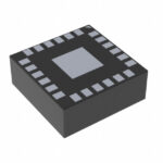 9FGV1004CQ551LTGI8
The activity of extra discounts on wholesale prices is in full swing…
Please fill in your contact information and we will send you the latest wholesale price list.





