ChipApex | Global Electronic Components Supplier
9FGV1005A002LTGI
Search Product
Search Post
— IC芯片 | 连接器 | 传感器 | 被动器件 —
Search productSearch post
— IC芯片 | 连接器 | 传感器 | 被动器件 —
Consult the customer manager about the wholesale price.
consultation hotline:86-132-6715-2157
email:[email protected]
Contact the product manager for consultation. One-stop consultation is available.
Do you want a lower wholesale price? Please send us your inquiry and we will reply immediately.
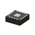
The 9FGV1005A002LTGI is a programmable PhiClock generator manufactured by Renesas Electronics. It operates within a supply voltage range of 1.71 V to 3.465 V and supports output frequencies up to 325 MHz. The device features an input frequency capability of up to 240 MHz and provides two outputs with LP-HCSL and LVDS signaling types. Packaged in a 16-LGA (3x3 mm) format with an exposed pad, it functions within a temperature range of -40°C to +85°C and draws approximately 24 mA during operation.
Verify the specific suffix 'A002' against official Renesas documentation to confirm factory-programmed parameters, as suffixes often denote fixed configuration or binning. Confirm the LGA-16 package dimensions and thermal pad requirements for PCB layout compatibility. Check current availability status through authorized distributors, as lead times may vary based on production schedules.
Select this component when a dual-output programmable clock solution is required for systems operating between 1.71 V and 3.465 V. Ensure the design accommodates the 16-TFLGA package footprint and thermal dissipation needs. Verify that the maximum 325 MHz output frequency meets the target application's bandwidth requirements and that LP-HCSL/LVDS output drivers are compatible with downstream receiver inputs.
This part belongs to the Renesas PhiClock 9FGV1005 series, designed for low-jitter clock generation in high-performance digital systems. The series offers programmability options to replace multiple fixed-frequency oscillators, reducing bill-of-materials complexity. The 9FGV1005 variant specifically targets applications requiring precise timing with flexible output configurations.
Direct substitutes within the same family include other 9FGV1005 variants with different output counts or pinouts, such as the 9FGV1005Q500LTGI. Cross-family replacements from other manufacturers require careful evaluation of electrical parameters, package dimensions, and jitter specifications to ensure functional equivalence.
 9FGV1005A002LTGI
The activity of extra discounts on wholesale prices is in full swing…
Please fill in your contact information and we will send you the latest wholesale price list.