ChipApex | Global Electronic Components Supplier
9FGV1005A211LTGI
Search Product
Search Post
— IC芯片 | 连接器 | 传感器 | 被动器件 —
Search productSearch post
— IC芯片 | 连接器 | 传感器 | 被动器件 —
Consult the customer manager about the wholesale price.
consultation hotline:86-132-6715-2157
email:[email protected]
Contact the product manager for consultation. One-stop consultation is available.
Do you want a lower wholesale price? Please send us your inquiry and we will reply immediately.
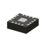
The 9FGV1005A211LTGI is a programmable clock generator from the Renesas PhiClock family. It operates with a single supply voltage ranging from 1.71V to 3.465V and supports input signals including HCSL, LVCMOS, LVDS, and crystals. The device features one internal phase-locked loop (PLL) circuit with a 1:4 input-to-output ratio. Maximum output frequency reaches 325MHz. Outputs are available in HCSL, LVCMOS, LVDS, and LVPECL formats. It functions within an ambient temperature range of -40°C to 85°C and utilizes a 16-TFLGA package with an exposed pad.
Verify the specific suffix 'A211' against official Renesas documentation to confirm factory configuration settings. Confirm moisture sensitivity level and reflow soldering profile requirements prior to assembly. Ensure ESD protection measures are implemented during handling due to the small form factor package.
Select this component when a single output channel with four differential or single-ended copies is required. Verify that the target application logic levels match the supported output types. Check if the 325MHz maximum frequency meets system bandwidth requirements. Consider the 16-TFLGA package constraints for PCB layout and thermal management.
This part belongs to the 9FGV1005 series, designed for low-jitter clock generation in high-performance computing environments. The PhiClock family emphasizes flexibility through programmable configurations and support for various industry-standard signaling interfaces.
Cross-reference with other 9FGV1005 variants such as 9FGV1005A004LTGI for pin-compatible alternatives. Verify electrical parameters and output configurations before substitution.
 9FGV1005A211LTGI
The activity of extra discounts on wholesale prices is in full swing…
Please fill in your contact information and we will send you the latest wholesale price list.