ChipApex | Global Electronic Components Supplier
9FGV1006A003LTGI
Search Product
Search Post
— IC芯片 | 连接器 | 传感器 | 被动器件 —
Search productSearch post
— IC芯片 | 连接器 | 传感器 | 被动器件 —
Consult the customer manager about the wholesale price.
consultation hotline:86-132-6715-2157
email:[email protected]
Contact the product manager for consultation. One-stop consultation is available.
Do you want a lower wholesale price? Please send us your inquiry and we will reply immediately.
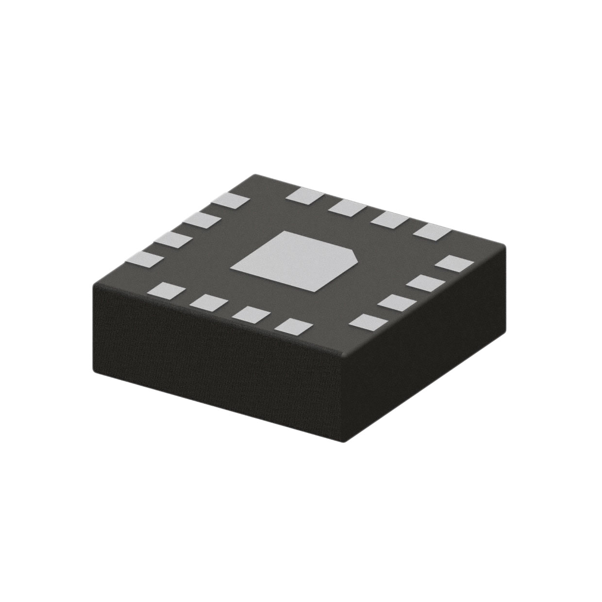
The 9FGV1006A003LTGI is a PhiClock™ programmable clock generator manufactured by Renesas Electronics. It operates within a supply voltage range of 1.71 V to 3.465 V and supports a maximum frequency of 325 MHz. The device features one circuit with a 1:4 input-to-output ratio, accepting HCSL, LVCMOS, LVDS, or crystal inputs. Outputs include HCSL, LVCMOS, LVDS, and LVPECL configurations. It utilizes an integer PLL architecture without fractional multiplication capabilities. The component is housed in a 16-TFLGA package with an exposed pad, suitable for surface mount installation across an operating temperature range of -40°C to 85°C.
Verify the specific suffix LTGI against the manufacturer's current datasheet to confirm pinout and electrical characteristics match the design requirements. Confirm moisture sensitivity level (MSL) and reflow soldering profile compatibility during assembly planning. Ensure I²C address settings align with system bus constraints if multiple devices are present.
Select this component when a single differential or single-ended input requires four matched output clocks with spread spectrum capability. Verify that the required output voltage levels (HCSL, LVCMOS, LVDS, LVPECL) are supported by the external termination network. Check that the 1.71 V to 3.465 V supply range matches the target system power rails.
This part belongs to the IDT/Renesas PhiClock™ programmable clock generator family, which was acquired by Renesas Electronics. The 9FGV1006 series offers factory-configurable options for output types and frequencies. The A003 suffix typically denotes a specific factory configuration regarding output signaling and frequency, distinct from other variants like C000.
Cross-reference with other 9FGV1006 variants such as 9FGV1006C000LTGI for identical package and function but different factory configurations. Ensure substitute parts maintain the same 16-TFLGA footprint and electrical specifications.
 9FGV1006A003LTGI
The activity of extra discounts on wholesale prices is in full swing…
Please fill in your contact information and we will send you the latest wholesale price list.