ChipApex | Global Electronic Components Supplier
9FGV1006A110LTGI8
Search Product
Search Post
— IC芯片 | 连接器 | 传感器 | 被动器件 —
Search productSearch post
— IC芯片 | 连接器 | 传感器 | 被动器件 —
Consult the customer manager about the wholesale price.
consultation hotline:86-132-6715-2157
email:[email protected]
Contact the product manager for consultation. One-stop consultation is available.
Do you want a lower wholesale price? Please send us your inquiry and we will reply immediately.
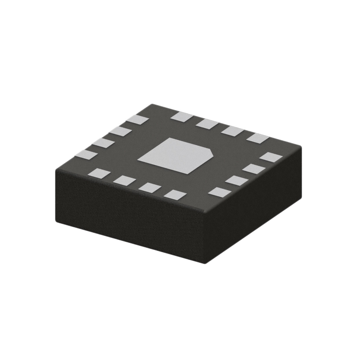
The 9FGV1006A110LTGI8 is a programmable clock generator from the Renesas PhiClock family, designed for high-performance timing applications. It features an integrated Phase-Locked Loop (PLL) and supports multiple input types including crystal, LVCMOS, LVDS, and HCSL. The device provides six differential outputs utilizing CML, HCSL, LP-HCSL, LVCMOS, LVDS, or LVPECL signaling standards. Operating within a supply voltage range of 1.71V to 3.465V across three domains, it functions reliably in temperatures from -40°C to 85°C. Packaged in a 16-TFLGA with an exposed pad, this component delivers precise clock distribution for complex digital systems.
Verify the specific suffix 'A110' against official Renesas documentation to confirm factory-programmed frequency settings and pinout variations. Confirm moisture sensitivity level (MSL) and reflow soldering profiles prior to assembly. Check for end-of-life status or alternative package recommendations if current stock is limited.
Select this component when six independent differential clocks are required from a single source. Ensure the target logic families match the supported output voltage levels (1.8V/2.5V/3.3V). Verify that the required output frequencies fall within the PLL multiplication/division capabilities defined in the datasheet. Consider thermal dissipation requirements due to the exposed pad design in the 16-LGA package.
This part belongs to the 9FGV1006 series, which offers configurable clock generation for high-speed serial interfaces. Unlike fixed-frequency buffers, the PhiClock family allows customization of output ratios via I2C or hardware pins. The LTGI8 suffix indicates a tape-and-reel packaging format suitable for automated surface-mount assembly.
Direct replacements include other members of the 9FGV1006 family such as the 9FGV1006Q550LTGI8, provided the programmed frequencies match. Cross-reference pinouts and electrical characteristics carefully, as programming configurations may differ between suffixes.
 9FGV1006A110LTGI8
The activity of extra discounts on wholesale prices is in full swing…
Please fill in your contact information and we will send you the latest wholesale price list.