ChipApex | Global Electronic Components Supplier
9FGV1006BQ507LTGI
Search Product
Search Post
— IC芯片 | 连接器 | 传感器 | 被动器件 —
Search productSearch post
— IC芯片 | 连接器 | 传感器 | 被动器件 —
Consult the customer manager about the wholesale price.
consultation hotline:86-132-6715-2157
email:[email protected]
Contact the product manager for consultation. One-stop consultation is available.
Do you want a lower wholesale price? Please send us your inquiry and we will reply immediately.
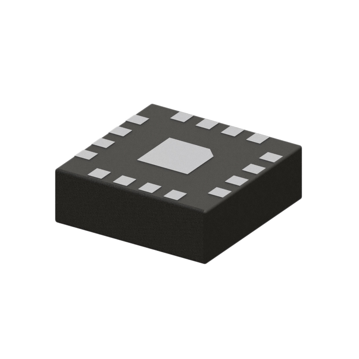
The Renesas 9FGV1006BQ507LTGI is a programmable PhiClock generator designed for high-speed digital interfaces. It operates within the PhiClock family, providing multiple output clock signals derived from a single input reference. The device supports LP-HCSL and LVDS output signaling standards, accommodating various logic families through AC coupling. Key electrical parameters include a core voltage of 1.8V and I/O voltages ranging from 1.8V to 3.3V. It features four differential outputs and two LVCMOS reference outputs, with an integrated crystal option available in specific configurations. The component is housed in a 24-lead LGA package measuring 4.0 x 4.0 mm.
Verify the specific suffix 'Q507' against official Renesas documentation to confirm factory-configured frequency settings. Ensure compatibility with the 24-LGA LTG24 package dimensions and Moisture Sensitivity Level 3 requirements during storage and assembly. Confirm lead-free status and RoHS compliance with current datasheets before procurement.
Select this component when designing systems requiring multiple synchronized clock outputs with low jitter for PCIe applications. Compare against the 9FGV1004 and 9FGV1002 models if different output counts or frequency ranges are needed. Verify that the required output signaling (LP-HCSL/LVDS) matches the target receiver inputs. Consider the integrated crystal feature if external oscillators are undesirable.
This part belongs to the Renesas PhiClock programmable clock generator family, which includes variants like the 9FGV1001, 9FGV1004, and 9FGV1008. These devices share common architectural features such as I2C configurability and spread-spectrum capabilities. The 9FGV1006 series specifically targets applications needing four differential outputs with flexible voltage levels, bridging the gap between simpler buffers and more complex multi-output generators.
Direct replacements within the same family include the 9FGV1004 and 9FGV1008, provided their factory-configured frequencies match the design requirements. Cross-model substitution requires verifying pinout compatibility and ensuring the alternative device supports the necessary PCIe generation jitter specifications.
 9FGV1006BQ507LTGI
The activity of extra discounts on wholesale prices is in full swing…
Please fill in your contact information and we will send you the latest wholesale price list.