ChipApex | Global Electronic Components Supplier
9FGV1006BQ508LTGI
Search Product
Search Post
— IC芯片 | 连接器 | 传感器 | 被动器件 —
Search productSearch post
— IC芯片 | 连接器 | 传感器 | 被动器件 —
Consult the customer manager about the wholesale price.
consultation hotline:86-132-6715-2157
email:[email protected]
Contact the product manager for consultation. One-stop consultation is available.
Do you want a lower wholesale price? Please send us your inquiry and we will reply immediately.
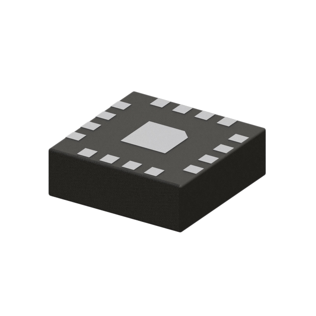
The 9FGV1006BQ508LTGI is a programmable PhiClock™ clock generator IC from Renesas Electronics Corporation. It utilizes a 16-TFLGA exposed pad package with dimensions of 3.0 x 3.0 x 1.1 mm and a 0.5 mm pitch. The device supports input frequencies ranging from 8 MHz to 50 MHz and provides output frequencies up to 325 MHz. It operates on supply voltages of 1.8 V, 2.5 V, or 3.3 V. Key electrical parameters include an RMS phase jitter of 0.276 ps and a maximum peak-to-peak core voltage jitter of 50 ps. The component features three outputs supporting LP-HCCL, LVCMOS, and LVDS signaling types.
Verify the specific suffix (e.g., LTGI) against official Renesas documentation to confirm package type and lead-free status. Confirm availability as this series may be subject to discontinuation notices. Ensure compatibility with required input crystal frequencies and output voltage levels before finalizing procurement orders.
Select this component when designing systems requiring precise, low-jitter clock signals for high-speed serial interfaces like PCIe. Consider the 16-LGA package constraints and thermal requirements. Verify that the fixed factory programming meets the exact frequency and protocol requirements, as user reprogramming is not supported after manufacturing.
This part belongs to the Renesas PhiClock™ series of programmable clock generators. These devices are designed to replace discrete oscillator solutions by providing flexible, multi-output clocking in a compact surface-mount package. The series targets high-performance computing and communication infrastructure where signal integrity is critical.
Consult official Renesas substitution lists for verified alternatives. Generic cross-references may not match the specific OTP programming or jitter specifications required for PCIe Gen5 compliance.
 9FGV1006BQ508LTGI
The activity of extra discounts on wholesale prices is in full swing…
Please fill in your contact information and we will send you the latest wholesale price list.