ChipApex | Global Electronic Components Supplier
9FGV1006CQ538LTGI8
Search Product
Search Post
— IC芯片 | 连接器 | 传感器 | 被动器件 —
Search productSearch post
— IC芯片 | 连接器 | 传感器 | 被动器件 —
Consult the customer manager about the wholesale price.
consultation hotline:86-132-6715-2157
email:[email protected]
Contact the product manager for consultation. One-stop consultation is available.
Do you want a lower wholesale price? Please send us your inquiry and we will reply immediately.
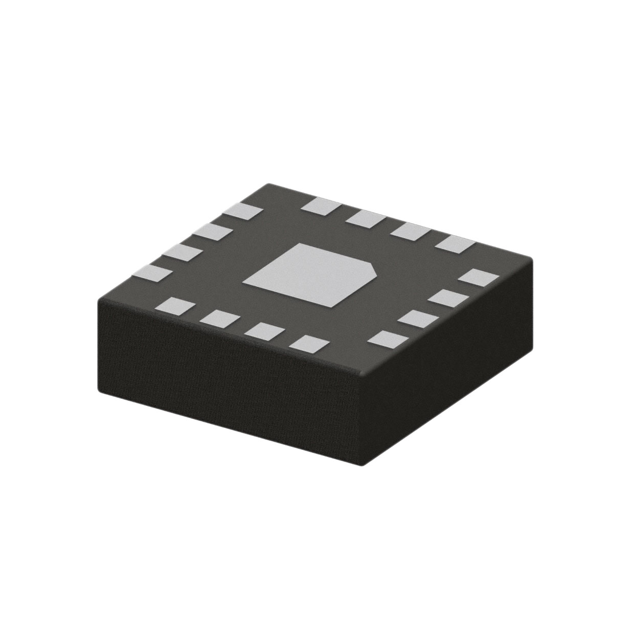
The 9FGV1006CQ538LTGI8 is a PhiClock programmable clock generator manufactured by Renesas Electronics. It operates with a supply voltage range of 1.71V to 1.89V, 2.375V to 2.625V, and 3.135V to 3.465V. The device supports input frequencies up to 200MHz and 325MHz, utilizing HCSL, LVCMOS, LVDS, or crystal inputs. Outputs include CML, HCSL, LP-HCSL, LVCMOS, LVDS, and LVPECL types. It features a 1:6 input-to-output ratio within a 16-TFLGA exposed pad package.
Verify component status as the specific variant may be listed as obsolete in certain distributor catalogs. Confirm moisture sensitivity level (MSL 3) and lead-free compliance prior to integration. Ensure ordering suffixes match exact packaging requirements such as tape and reel quantities. Cross-reference datasheet revisions to confirm pinout and electrical parameter consistency against current design specifications.
Select this component when designing systems requiring strict phase jitter compliance for multiple PCIe generations. The device offers flexible output voltage levels and signaling types suitable for mixed-voltage environments. Consider the 16-LGA package dimensions for PCB layout constraints. Verify that the required input frequency range aligns with available crystal or oscillator sources.
This part belongs to the Renesas PhiClock series of clock generators. It is designed to provide precise timing signals for complex digital systems. The series typically includes variants with different output configurations and frequency ranges. These devices are commonly used in server, storage, and networking equipment requiring low-jitter clock distribution.
Public confirmed substitute part numbers include 9FGV1006A110LTGI8 and 9FGV1006A202LTGI8. Verify functional equivalence regarding output ratios and supported PCIe generations before substitution.
 9FGV1006CQ538LTGI8
The activity of extra discounts on wholesale prices is in full swing…
Please fill in your contact information and we will send you the latest wholesale price list.