 ChipApex | Global Electronic Components Supplier
9SQL4954BNLGI8
Search Product
Search Post
— IC芯片 | 连接器 | 传感器 | 被动器件 —
Search productSearch post
— IC芯片 | 连接器 | 传感器 | 被动器件 —
Consult the customer manager about the wholesale price.
consultation hotline:86-132-6715-2157
email:[email protected]
Contact the product manager for consultation. One-stop consultation is available.
Do you want a lower wholesale price? Please send us your inquiry and we will reply immediately.
The 9SQL4954BNLGI8 is a clock generator from the IDT 'Lite' family, manufactured by Renesas Electronics. It generates four 100MHz outputs designed to exceed CK420BQ requirements for server applications. The device supports PCIe Common Clock and Independent Reference architectures with integrated 85Ω terminations. Key specifications include cycle-to-cycle jitter under 50ps, output-to-output skew under 50ps, and phase jitter below 2ps rms (12k-20M). It operates on a 3.135V to 3.465V supply within an industrial temperature range of -40°C to 85°C.
Verify the component's origin as IDT products are now managed by Renesas Electronics. Confirm that the specific ordering suffix matches the required package and environmental specifications. Ensure compatibility with the SMBus interface if dynamic configuration is needed for the device.
Select this component when designing systems requiring low-power HCSL outputs with integrated impedance matching to reduce external components. It is suitable for applications needing multiple independent clock outputs with individual enable controls and support for various PCIe clock architectures.
This part belongs to the 9SQL49xx series, specifically derived from the CK420BQ architecture. It is marketed as a 'Lite' family solution offering reduced power consumption compared to its predecessor while maintaining compliance with high-speed serial interface standards.
Direct replacements should be sought within the 9SQL49xx series or compatible CK420BQ derivatives. Verify pinout and electrical characteristics match before substitution.
The 12kHz to 20MHz phase jitter is typically 2ps rms with Spread Spectrum Clocking (SSC) turned off.
The SMBus address is latched based on the state of the SADR pin when the CKPWRGD_PD# signal is first asserted high.
Yes, the 25MHz REF output supports Wake-On-LAN mode, allowing the reference clock to remain active during power-down states.
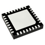 9SQL4954BNLGI8
The activity of extra discounts on wholesale prices is in full swing…
Please fill in your contact information and we will send you the latest wholesale price list.






