 ChipApex | Global Electronic Components Supplier

SEARCH
Search Product
Search Post
— IC芯片 | 连接器 | 传感器 | 被动器件 —
Search productSearch post
— IC芯片 | 连接器 | 传感器 | 被动器件 —
Consult the customer manager about the wholesale price.
consultation hotline:86-132-6715-2157
email:[email protected]
Contact the product manager for consultation. One-stop consultation is available.
Do you want a lower wholesale price? Please send us your inquiry and we will reply immediately.
A1010B-2PLG68I is listed in the Field Programmable Gate Array range at ChipApex. The manufacturer field lists Microsemi Corporation. Its product description is IC FPGA 57 I/O 68PLCC. Review the specifications below when checking this part for your BOM.
The A1010B-2PLG68I is a field-programmable gate array (FPGA) from the ACT™ 1 series, manufactured by Microsemi Corporation. It features 1200 gate array equivalent gates and 295 programmable logic modules. The device operates within an industrial temperature range of -40°C to +85°C and utilizes a 68-pin plastic leaded chip carrier package. Key electrical specifications include a supply voltage range of 4.5V to 5.5V for the 5V family, with maximum data rates reaching 75 MHz. It supports up to 57 user I/Os and includes two in-circuit diagnostic probe pins.
Verify component authenticity through authorized distributors or direct manufacturer channels. Confirm that the specific ordering suffix matches the required speed grade and application temperature range. Ensure compliance with relevant export control classifications and environmental standards prior to acquisition.
Select this model when 1200 gate capacity and 57 I/Os are sufficient for the target design. The '2' speed grade offers approximately 25% faster performance than standard speed variants. Choose this package only if the board layout accommodates the 68-pin plastic leaded chip carrier form factor.
This component belongs to the ACT™ 1 FPGA family, which employs 1.0 micron CMOS technology. The family includes variants such as A1020B for higher density and A10V10B for 3.3V operation. These devices share common architectural features including the PLICE antifuse process and diagnostic probe capabilities.
Direct functional replacements within the same package and pinout may include other ACT 1 series devices like the A1010B-1PLG68I or A1010B-3PLG68I, depending on required speed grades. Verify compatibility with existing design tools and programming hardware before substitution.
The MODE pin controls multifunction pins such as DCLK and SDI. When HIGH, special functions are active; when LOW, these pins function as general I/O.
It uses patented PLICE antifuses with low resistance and capacitance. The architecture limits antifuses per path to a maximum of four, ensuring tight fanout delay distributions.
No, unused I/O pins are automatically driven LOW by the ALS software to prevent undefined states and excessive current draw.
Explore related parts through Embedded, Integrated Circuits (ICs), all product categories, ChipApex homepage.
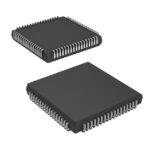 A1010B-2PLG68I

The activity of extra discounts on wholesale prices is in full swing…
Please fill in your contact information and we will send you the latest wholesale price list.





