 ChipApex | Global Electronic Components Supplier

SEARCH
Search Product
Search Post
— IC芯片 | 连接器 | 传感器 | 被动器件 —
Search productSearch post
— IC芯片 | 连接器 | 传感器 | 被动器件 —
Consult the customer manager about the wholesale price.
consultation hotline:86-132-6715-2157
email:[email protected]
Contact the product manager for consultation. One-stop consultation is available.
Do you want a lower wholesale price? Please send us your inquiry and we will reply immediately.
A3P400-2FGG484I is listed in the Field Programmable Gate Array range at ChipApex. The manufacturer field lists Microsemi Corporation. Its product description is IC FPGA 194 I/O 484FBGA. Review the specifications below when checking this part for your BOM.
The A3P400-2FGG484I is a ProASIC3 Flash Field Programmable Gate Array featuring 400,000 system gates and 9,216 VersaTiles. It utilizes a 130-nm flash-based CMOS process with a maximum operating frequency of 350 MHz. The device supports up to 54 kbits of embedded dual-port SRAM and includes one integrated PLL within its six Clock Conditioning Circuits. It operates at a core voltage of 1.5 V and provides 194 user I/Os in an FG484 Fine Pitch Ball Grid Array package measuring 23 mm by 23 mm. The 'I' suffix designates an industrial temperature range from -40°C to +100°C.
Verify the specific speed grade indicated by the '2' suffix, which denotes performance faster than standard variants. Confirm that the FG484 package dimensions align with your PCB footprint requirements. Ensure the industrial temperature rating meets your environmental specifications. Check current availability status as legacy flash FPGA lines may have limited production runs.
Select this device when nonvolatile configuration and immediate system startup are critical requirements. Consider the 400,000 gate capacity for moderate complexity designs needing low static power consumption. Evaluate the 194 available I/Os against your interface needs before choosing smaller packages like FG256 or larger densities like A3P600.
This component belongs to the Microsemi ProASIC3 Flash family, representing third-generation flash FPGA technology. It bridges the gap between CPLDs and high-density SRAM FPGAs by offering ASIC-like unit costs with FPGA reprogrammability. The family emphasizes security and instant-on capabilities for cost-sensitive applications.
For pin-compatible upgrades within the same package, consider the A3P600 or A3P1000 series devices. Higher density options provide increased logic resources while maintaining the FG484 footprint. Verify software toolchain compatibility if migrating to newer ProASIC3E or SmartFusion families.
No, the device uses nonvolatile flash technology, allowing it to boot instantly without external configuration memory components.
The '2' indicates a speed grade that is 25% faster than the standard speed grade (blank) variant of the A3P400 device.
The device contains six CCC blocks, with one block integrating a Phase-Locked Loop (PLL) for clock synthesis.
Explore related parts through Embedded, Integrated Circuits (ICs), all product categories, ChipApex homepage.
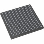 A3P400-2FGG484I

The activity of extra discounts on wholesale prices is in full swing…
Please fill in your contact information and we will send you the latest wholesale price list.





