 ChipApex | Global Electronic Components Supplier

SEARCH
Search Product
Search Post
— IC芯片 | 连接器 | 传感器 | 被动器件 —
Search productSearch post
— IC芯片 | 连接器 | 传感器 | 被动器件 —
Consult the customer manager about the wholesale price.
consultation hotline:86-132-6715-2157
email:[email protected]
Contact the product manager for consultation. One-stop consultation is available.
Do you want a lower wholesale price? Please send us your inquiry and we will reply immediately.
The A40MX02-2PL68I is a field-programmable gate array (FPGA) from the Microchip MX series, manufactured by Microchip Technology. It features 295 logic elements and approximately 3,000 system gates. The device provides 57 input/output pins and operates within a supply voltage range of 4.5 V to 5.5 V, supporting both 3.3 V and 5 V core voltages. It is housed in a PLCC-68 surface-mount package and functions reliably across an industrial temperature range of -40°C to +85°C.
Verify the specific suffix 'I' confirms the industrial temperature grade (-40°C to +85°C) against the official datasheet. Confirm the PLCC-68 package type matches the design footprint. Check current RoHS compliance status and moisture sensitivity level requirements before integration into the manufacturing process.
Select this component when a low-gate-count FPGA with mixed-voltage support is required. Ensure the design utilizes the 57 available I/Os efficiently. Consider the PLCC-68 package constraints for PCB layout. Verify that the 3.3V or 5V operating modes align with the system power architecture.
This part belongs to the A40MX02 family, which offers 3,000 to 54,000 system gates. The MX series is designed as a high-capacity alternative to ASICs, featuring fast wide-decode circuitry and configurable dual-port SRAM resources for complex logic implementations.
Direct substitutes include other variants within the A40MX02 family, such as the A40MX02-2PQG100 for different pin counts or the A40MX02-VQG80M for extended temperature ranges. Cross-reference package dimensions and electrical specifications carefully.
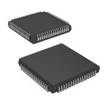 A40MX02-2PL68I

The activity of extra discounts on wholesale prices is in full swing…
Please fill in your contact information and we will send you the latest wholesale price list.





