 ChipApex | Global Electronic Components Supplier

SEARCH
Search Product
Search Post
— IC芯片 | 连接器 | 传感器 | 被动器件 —
Search productSearch post
— IC芯片 | 连接器 | 传感器 | 被动器件 —
Consult the customer manager about the wholesale price.
consultation hotline:86-132-6715-2157
email:[email protected]
Contact the product manager for consultation. One-stop consultation is available.
Do you want a lower wholesale price? Please send us your inquiry and we will reply immediately.
The A40MX02-2PLG44I is a Field Programmable Gate Array (FPGA) from the Microchip MX series, manufactured by Microchip Technology. It features 295 Configurable Logic Blocks (CLBs) and approximately 3,000 system gates. The device supports mixed-voltage operation with supply ranges of 3.0V to 3.6V for 3.3V core applications and 4.75V to 5.25V for 5.0V core applications. It is housed in a 44-pin PLCC package and operates within an industrial temperature range of -40°C to +85°C.
Verify the specific suffix 'I' confirms the industrial temperature grade (-40°C to +85°C). Confirm the package type is PLCC-44. Check RoHS compliance status as required by project specifications. Ensure ESD handling procedures are followed due to moisture sensitivity level 3 classification.
Select this component when 3,000 system gates and 44 I/O pins are sufficient for the design. Choose the 'I' suffix for industrial temperature requirements over commercial grades. Consider the PLCC-44 package constraints regarding PCB space and thermal dissipation compared to QFP or BGA alternatives.
This part belongs to the A40MX02 family within the broader MX FPGA portfolio. It shares architectural similarities with other devices like the A40MX04 but offers lower gate density. The family is known for fast wide-decode circuitry and configurable dual-port SRAM capabilities.
Direct substitutes include other parts within the A40MX02 family such as A40MX02-2PQG100 for different pin counts. Cross-family replacements may require significant schematic and layout modifications due to differences in I/O configurations and logic block architectures.
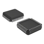 A40MX02-2PLG44I

The activity of extra discounts on wholesale prices is in full swing…
Please fill in your contact information and we will send you the latest wholesale price list.






