 ChipApex | Global Electronic Components Supplier

SEARCH
Search Product
Search Post
— IC芯片 | 连接器 | 传感器 | 被动器件 —
Search productSearch post
— IC芯片 | 连接器 | 传感器 | 被动器件 —
Consult the customer manager about the wholesale price.
consultation hotline:86-132-6715-2157
email:[email protected]
Contact the product manager for consultation. One-stop consultation is available.
Do you want a lower wholesale price? Please send us your inquiry and we will reply immediately.
The A40MX02-FPLG68 is a Field Programmable Gate Array from the Microchip MX family, designed as a high-capacity single-chip ASIC alternative. It features 295 Logic Elements and approximately 3,000 system gates. The device operates with a supply voltage range of 4.5 V to 5.5 V and supports mixed-voltage I/O configurations at 3.3 V or 5.0 V. It provides 57 user-programmable I/O pins within a 68-pin PLCC package. The component supports an industrial temperature range from -40°C to +85°C.
Verify the specific suffix 'F' against official Microchip documentation to confirm it denotes the industrial temperature grade (-40°C to +85°C). Confirm the package type corresponds to the 68-lead Plastic Leadless Chip Carrier (PLCC). Ensure compliance with RoHS directives and check for any recent Production Change Notices regarding assembly sites or material updates before finalizing procurement.
Select this component when a design requires approximately 3,000 system gates with mixed-voltage I/O flexibility. It is suitable for applications needing deterministic timing and in-system diagnostics. Compare against other MX series variants if higher gate counts or different package options are required. Verify that the 57 available I/O pins meet the interface requirements of the target system.
This part belongs to the A40MX02 series within the broader MX FPGA family produced by Microchip Technology. The family ranges from 3,000 to 54,000 system gates and includes configurable dual-port SRAM. The A40MX02 variant specifically targets low-to-medium complexity logic replacement tasks, offering a cost-effective alternative to custom ASICs while maintaining high reliability and ease of integration.
Direct substitutes include other parts in the A40MX02 series with compatible packages, such as A40MX02-PLG68I. Cross-reference pinouts and electrical characteristics carefully when considering alternatives from other manufacturers, as architecture differences may impact performance and compatibility.
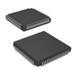 A40MX02-FPLG68

The activity of extra discounts on wholesale prices is in full swing…
Please fill in your contact information and we will send you the latest wholesale price list.







