 ChipApex | Global Electronic Components Supplier

SEARCH
Search Product
Search Post
— IC芯片 | 连接器 | 传感器 | 被动器件 —
Search productSearch post
— IC芯片 | 连接器 | 传感器 | 被动器件 —
Consult the customer manager about the wholesale price.
consultation hotline:86-132-6715-2157
email:[email protected]
Contact the product manager for consultation. One-stop consultation is available.
Do you want a lower wholesale price? Please send us your inquiry and we will reply immediately.
The A40MX04-3PQ100 is a field-programmable gate array (FPGA) from the Microsemi MX family, manufactured by Microchip Technology. It features 295 Configurable Logic Blocks (CLBs) and approximately 2000 equivalent system gates. The device supports a maximum clock frequency of 48.24 MHz with a CLB propagation delay of 3.72 ns. It operates within an industrial temperature range of -55°C to +125°C and utilizes a 100-pin Plastic Quad Flat Package (PQFP). The FPGA requires dual voltage supplies: 3V to 3.6V for core logic and 4.75V to 5.25V for I/O interfaces.
Verify the specific suffix designation against official Microchip documentation to confirm package type and temperature grade. Ensure compatibility with existing PCB footprints for the 100-pin PQFP variant. Confirm moisture sensitivity level handling requirements during assembly processes to prevent damage.
Compare the A40MX04-3PQ100 with other MX series devices based on I/O count and logic density requirements. Evaluate power consumption profiles against alternative SRAM-based FPGAs if non-volatility is not critical. Assess thermal management needs given the wide operating temperature range and package thermal characteristics.
This component belongs to the Microsemi 40MX/42MX FPGA family, designed for cost-sensitive applications requiring robust performance. The MX series is characterized by its flash-based technology, which eliminates the need for boot PROMs and reduces overall system complexity and bill of materials.
Direct pin-to-pin replacements within the same package may include other speed grades or temperature variants of the A40MX04 series, such as the A40MX04-1PQ100 or A40MX04-2PQ100, provided timing constraints are met. Cross-family migration to PolarFire or IGloo2 requires schematic and layout redesign.
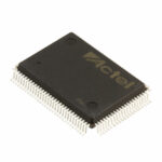 A40MX04-3PQ100

The activity of extra discounts on wholesale prices is in full swing…
Please fill in your contact information and we will send you the latest wholesale price list.






